Dynamic Modulation of Plasmonic Structures
Hans Dyrnesli1, Gunnar Klös1, Matteo Miola2
and Duncan S. Sutherland1, *
1iNANO Center, University of Aarhus, Aarhus 8000, Denmark
2Carbon Dioxide Activation Center (CADIAC), iNANO Center,
University of Aarhus, Aarhus 8000, Denmark
E-mail: duncan@inano.au.dk
*Corresponding Author
Received 30 October 2018; Accepted 30 January 2019;
Publication 20 February 2019
Journal of Self-Assembly and Molecular Electronics, Vol. 7_1, 1–22.
doi: 10.13052/jsame2245-4551.7.001
This is an Open Access publication. © 2019 the Author(s). All rights reserved.
Abstract
A method for active switching of plasmonic structures by surface oxide-stabilized silver deposition is presented. The longitudinal dipole mode in pairs of closely spaced gold nanodisks on ITO was switched by depositing and removing a connecting layer of silver in solution. Optical properties were studied using VIS-NIR extinction spectroscopy and confirmed by FDTD simulations. Uniform dimensional growth by selective silver deposition brought pairs of gold nanodisks of 73 nm average diameter and 11 nm average distance into electrical contact. The growth process was studied by spectroelectrochemical measurements, and uniformity and selectivity were confirmed by SEM and XPS analysis, respectively. Uniform deposition was achieved by introduction of surface oxides on immobilized gold nanodisks, and selectivity by undervoltage deposition. Deposition of silver on disk pairs caused a blue-shift of the transverse dipole mode resonance of roughly 50 nm, and emergence of a new longitudinal mode with resonance around 960 nm. These results demonstrate the possibility for not only tuning of resonance peak position, but also on-demand switching of an additional mode which can provide materials with switchable optical properties.
Keywords: Nanofabrication, active plasmonics, silver electrodeposition, gold nanoparticles, hole-mask colloidal lithography
1 Introduction
Metal and semiconductor nanoparticles have attracted significant research attention in the recent decades because of their simplicity and unique optical properties. Specifically noble metal nanoparticles have found widespread application as contrast agents in scanning (SEM) and transmission (TEM) electron microscopy, due to their intrinsic high secondary-electron emission yield [1, 2], as colorants in bioimaging [3, 4] and ELISA-type biosensing assays [5], and in the past as antibody-linked gold nanospheres in pregnancy tests [6], because of their strong interaction with visible light. These interactions are dominated by resonant oscillations of conduction band electrons in the dimensionally confined metal nanoparticles, driven by the electric field component of incident electromagnetic radiation, known as localized surface plasmon resonances (LSPRs). For noble metal nanoparticles, energy conditions for LSPR are generally met in the UV-VIS-NIR region. The confined nature of LSPR and the strong local field enhancement allows manipulation of light below the diffraction limit, a property being actively researched for potential application in nanolenses, waveguides, and highly localized refractive index sensing [7–10]. LSPR energy depends on the nanoparticles material electronic properties, shape, size, inter-particle coupling and local dielectric environment [11]. Control of these parameters form the basis of the field of active plasmonics. Active plasmonics is a relatively new subfield of plasmonics, emerging as a result of the increased understanding of the working principle of plasmonics and advancements in manufacturing techniques, allowing active control over plasmonic properties. At its core, active plasmonics consists of plasmonic structures with optical properties controllable by external stimuli in a reversible fashion. Control parameters can include inter-particle distance, carrier control, and control of dielectric environment. Several control methods have recently been proposed, notably: mechanical control of inter-particle spacing [12], switchable coupling of Au-Ag/AgCl core-shell dimers [13], and tuneable plasmon resonance by silver deposition on gold nanostars [14]. In the present work, we demonstrate quasi-reversible active plasmon control through surface-oxide stabilized selective electrochemical undervoltage deposition of silver on weakly coupled gold nanodisk dimers, resulting in appearance and disappearance of modes in the near-infrared. Spectroelectrochemical analysis was carried out on a well-characterized single-disk system, and this method was applied to bring adjacent gold nanodisk into electrical contact by uniform dimensional growth. The presented method conveniently utilizes the combination of plasmonics and electrochemistry on a single substrate that has application in optical switching.
2 Experimental
All solvents and chemicals were purchased from Sigma Aldrich (Denmark), unless otherwise stated, and were of analytical grade. Solutions were prepared using ultra pure water (MQ, resistivity >18 MΩ·cm).
2.1 Nanostructure Fabrication
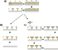
Gold disks with a nominal diameter of 100 nm were deposited on ITO-coated borosilicate glass slides (Deposition Research Lab, USA) using a standard hole-mask colloidal lithography (HCL) method. Briefly, 160–180 nm of A495 poly(methyl methacrylate) (PMMA) was spun-coated onto ITO-glass followed by sequential adsorption and drying of three layers of polyelectrolytes (poly(diallyldimethylammonium chloride) (PDDA) 2%, poly(styrenesulfonate) (PSS) 2% and polyaluminium chloride (PAX-XL60, Kemira Miljø, Denmark) 5%, all in MQ). Sulfonated polystyrene particles (0.2% by weight in MQ) of 0.1 μm nominal size (Invitrogen, Denmark) were brought to self-assemble onto the surface for 2 minutes, and excess particles were removed by thorough rinsing with MQ. Once dried under a stream of nitrogen, a 20-nm sacrificial titanium mask was deposited by physical vapour deposition (PVD) electron beam induced thermal evaporation (Cryofox GLAD, Polyteknik Denmark). Titanium-capped polystyrene particles were removed by tape-stripping, and oxygen plasma (RF power 50 W, 25 mbar, 40 sccm oxygen) was used to etch exposed PMMA down to the ITO-coated glass substrate (Figure 1(a)). Through the mask, 20 nm gold was evaporated via PVD at normal angle and the mask removed by sequential sonication in acetone, ethanol, and MQ, leaving gold disks with a nominal diameter of 100 nm and a height of 20 nm on the substrate surface (Figure 1(b)).
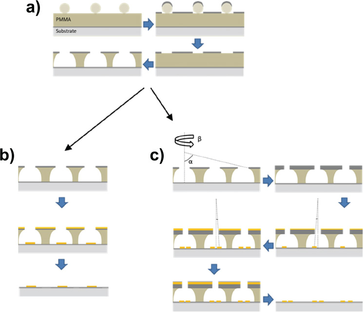
Figure 1 Schematic representation of nanodisks fabrication. a), polystyrene particles were immobilized on substrate by self-assembly, followed by titanium deposition, tape-stripping and plasma etching. b), For single-disk functionalization, gold was deposited at normal angle followed by mask removal. c), For disk-pair functionalization, hole-mask diameter was reduced by titanium deposition at 70° while rotating the substrate, followed by two stationary depositions at 14° and –14°, respectively, and subsequent mask removal.
Closely spaced pairs of gold nanodisks were fabricated by first shrinking the holes in the titanium hole-mask by means of glancing angle deposition [15] of 45 nm titanium at an angle of α = 70° while rotating the substrate. 20 nm gold was subsequently deposited without substrate rotation at α-angles of 14° and –14°, respectively, and the hole mask was removed as described above (Figure 1(c)).
2.2 Silver Electrodeposition
All electrochemical measurements were made using an Ivium CompactStat in a three-electrode configuration. Electrodes (bare ITO and nanodisk-functionalized ITO) were cleaned by sequential ultrasonication in acetone, ethanol and MQ for 10 minutes each, and dried in a stream of nitrogen. The clean electrodes were transferred to a 50-ml electrochemical cell and used as working electrodes without further preparation. Surface oxide formation on the gold disks was carried out by oxidation under stirring in 50 mM NaOH at +1.25 V for 2 minutes and in 50 mM H2SO4 at +1.35 V for 2 minutes. Silver deposition was performed at –50 mV for 135 seconds in a 1 M NH3 solution containing 500 μM AgNO3. Deposited silver was removed by scanning between –50 mV and +400 mV at 50 mV/s for 10 cycles in 1 M NH3 under stirring.
2.3 Characterization
Characterization of gold disks before and after silver deposition was carried out by SEM analysis (FEI Magellan 400, 5 kV, and 50 pA emission current). All stated dimensions were established using ImageJ with high-contrast SEM images. Surface composition was examined using XPS (Kratos AXIS Ultra DLD). The detector pass energy was 20 eV and 120 eV for survey and high resolution scans, respectively. Spectral deconvolution was performed using CasaXPS. Optical spectra were recorded using a fiber-coupled photodiode array spectrophotometer (BWTek Cypher H) with an unpolarised tungsten light source (BWTek BPS2.0). Three separate samples of disk-pair functionalized ITO samples were used in this study and results from one is presented here.
2.4 Simulation
Simulations were performed with the Finite-Difference Time-Domain (FDTD) solver from Lumerical Solutions (Canada). The dielectric functions of Ag and Au are taken from Johnson & Christy [16]. ITO substrate was included in all simulations, and the dielectric function was taken from [17]. For the simulations without Ag, a minimum mesh size of 2 × 2 × 2 nm3 was used, with Ag, it was reduced to 0.1 × 0.1 × 0.1 nm3 for stability reasons, in both cases with perfectly matched layer boundary conditions.
3 Results and Discussion
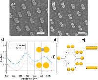
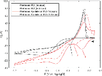
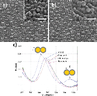
The intended system was first conceptualized using a system of closely spaced gold nanodisks connected by a silver bridge (Figure 2(a)). The silver bridge was non-reversibly removed by wide-potential cyclic voltammetry (CV) in 50 mM H2SO4 (CV data not shown) (Figure 2(b)). Optical spectra of the connected and non-connected disk pairs, along with schematic illustrations, are shown in Figure 2(c). The observed shift between the pink and blue curves is likely due to a combination of light interacting with the silver bridges, and sulphuric acid etching the ITO substrate. The shape of the extinction spectrum for the connected disk pairs resembles that of nanorods, with the high and low energy peaks stemming from transverse and longitudinal plasmon modes, respectively [18] (Seen schematically in Figure 2(e)).
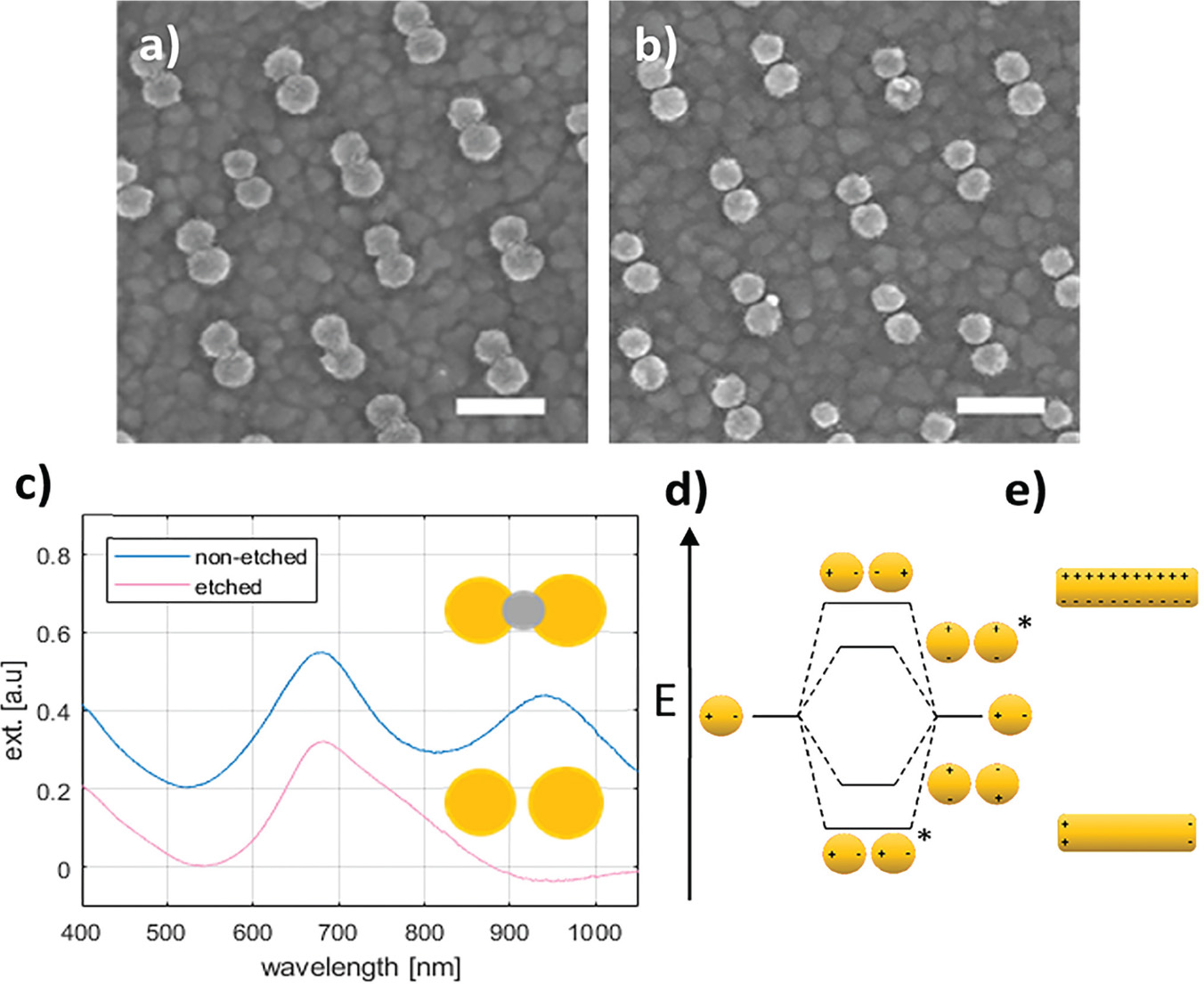
Figure 2 Etching of silver-bridged gold nanodisk pairs. SEM images of pair of roughly 80 nm diameter gold disks connected by a silver bridge before (a) and after (b) etching. c), optical spectra of bridged gold disks before (blue curve) and after (pink curve) etching. d), schematic representation of plasmon hybridization showing splitting of energy levels for coupled nanostructures. Stars indicate excitable bright modes. e), schematic illustration of energy difference between transverse (upper) and longitudinal (lower) modes in gold nanorods. Scale bars are 200 nm.
The asymmetry of the peak observed for the non-connected gold disk pairs in Figure 2(c) results from a difference in the diameter of the disks in the disk pair combined with hybridisation effects [19]. The difference in diameter of the two disks arises from the hole-mask process used where material deposited on the mask itself will cause a shrinkage of the hole proportional to the amount of material deposited. This effect is responsible for the slight vertical tapering observed for structures fabricated using HCL [15], but also results in the small difference in diameter between the first and second disks to be deposited in each disk pairs seen in Figure 2(a) and (b). The plasmon resonance for individual disks is systematically red shifted for increasing diameter disks [20]. The second contributing effect is described by plasmon hybridisation theory [19]. The close proximity of the gold nanodisks in a pair allows for coupling of LSPR modes, giving an energy splitting into multiple modes (Figure 2(d)). The peak shape is dominated by the lower energy, polarization-dependent bonding modes responsible for the tapering towards longer wavelengths [21–23]. The inhomogeneous broadening caused by variation in individual disk diameters (see Figure 6(a)) and wall to wall disk spacings (11.2 nm ± 6.0 nm, data not shown) manifests itself as the broad near-infrared tail seen in Figure 2(c). The multiple hybridised modes shown in Figure 2(d) can be split into symmetric or bright modes with both dipoles oriented in parallel (indicated with stars in Figure 2(d)) and in phase or anti-symmetric or dark modes with dipoles out of phase. The effect of the anti-symmetric, or dark modes, is negligible here, as the low net dipole moment modes are poorly excited by normal incident planar waves.
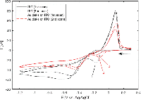
Electrodeposition of silver from solution under various conditions has been extensively studied as a means of altering the optical and electrical properties of ITO-coated substrates [24–26]. However, in the present study this is undesirable, as absorption and scattering from non-specifically deposited silver particles on ITO would obscure the optical signal from the gold nanostructures. In order to establish appropriate conditions for selective deposition of a uniform layer of silver onto the gold nanodisks, wide-potential CV curves were recorded for bare ITO- and gold nanodisk-functionalized ITO-coated substrates in an aqueous 1 M NH3 solution containing 500 μM AgNO3 (Figure 3).
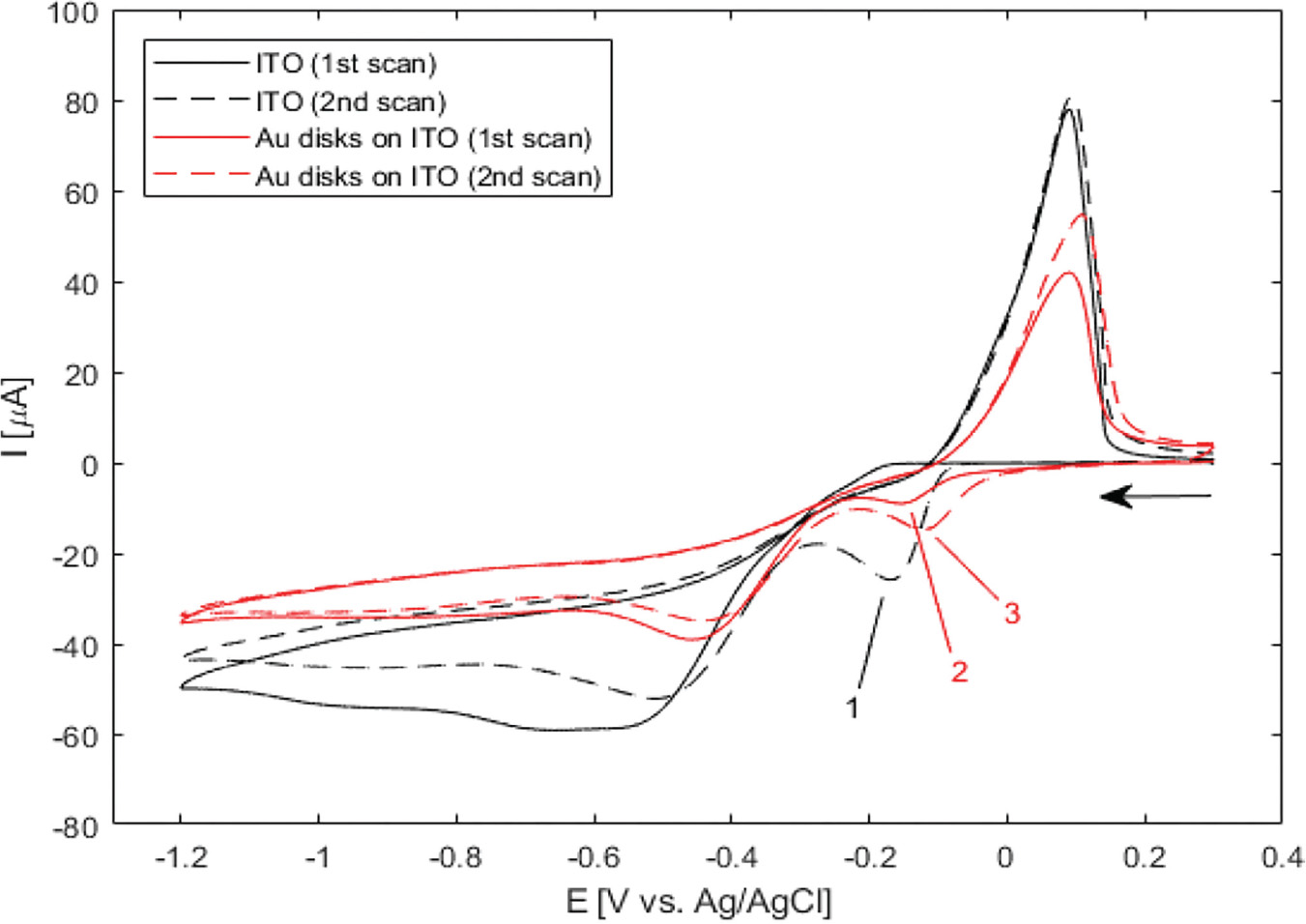
Figure 3 Wide-potential cyclic voltammograms of bare ITO and nanodisk-functionalized ITO (black and red curves, respectively) between +0.3 V and –1.2 V at 50 mV/s in 1 M NH3 containing 500 B5M AgNO3. Markers show locations of reduction of silver in the cathodic half-wave of bare ITO (–169 mV, second scan (1)) and nanodisk-functionalized ITO (–156 mV first scan, –122 mV second scan, (2) and (3), respectively). Arrow indicates scan direction.
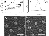
In the CV curve of the second scan for bare ITO a peak appears in the cathodic half-wave around –170 mV, not present in the first scan (1 in Figure 3) indicating deposition of silver. This observation suggests that nucleation sites for silver deposition at ITO can be created at large negative potentials in the first cycle, which lower the potential of the reduction process in the following cycles. This behaviour was not observed for gold nanodisk-functionalized ITO, where the gold disks likely function as nucleation sites for silver at low negative potentials, being further stabilized after first scan (2 and 3 in Figure 3, respectively). The apparent difference in deposition mechanism observed suggested a potential-based method for selectively depositing silver on gold nanodisks. Indeed, for deposition at a static potential of –50 mV for 45 seconds, electrochemical stripping analysis showed a more than 400-fold increase in the amount of silver deposited on gold nanodisk-functionalized ITO compared to bare ITO (Figure 4(a) and (b)). However, SEM images show a non-uniform growth pattern, resembling growth of single isolated nucleation sites (Figure 4(c) and (d)). Localized deposition is promoted by sharp points and edges on the nanodisks where the field is concentrated, an effect similar to that reported by Chimera et al. for silver deposition on gold nanocrystals [12].

Figure 4 Top: stripping assay of silver deposition on bare ITO and nanodisk-functionalized ITO after deposition for 45 seconds at –50 mV in 1 M NH3 containing 500 μM AgNO3. Integrated charge for deposition on bare ITO was 0.247 μC (a) and 103 μC for nanodisk-functionalized ITO (b). Bottom: Comparison of disk morphology before (c) and after (d) silver deposition. Scale bars are 200 nm.
D. Hernández-Santos et al. proposed a method for determining surface area of colloidal gold nanoparticles adsorbed on a carbon paste electrode using selective silver electrodeposition and subsequent stripping [27]. Briefly, colloidal gold nanoparticles were sequentially oxidized in basic and acidic media and silver was co-reduced onto the gold nanoparticles at a slightly negative potential and was reported to give homogeneous silver deposition on gold. This method was adapted here with small modifications, and the results of wide-potential cyclic voltammetry are shown in Figure 5.
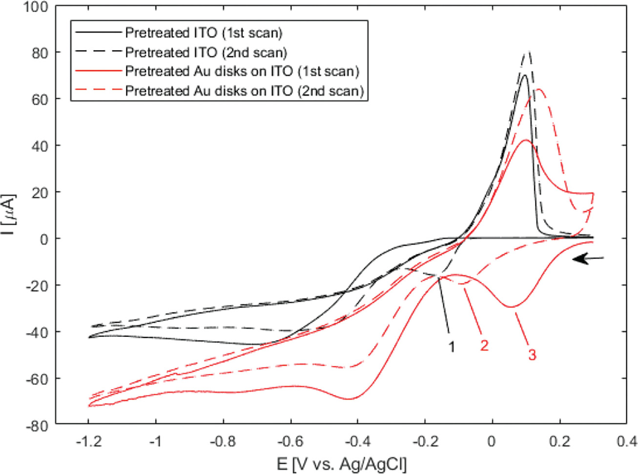
Figure 5 Wide-potential cyclic voltammograms of pretreated bare ITO and nanodisk-functionalized ITO (black and red curves, respectively) between +0.3 V and –1.2 V at 50 mV/s in 1 M NH3 containing 500 B5M AgNO3. Markers show locations of reduction of silver in the cathodic half-wave of bare ITO (–174 mV, second scan (1)) and nanodisk-functionalized ITO (+56 mV first scan, –93 mV second scan, (2) and (3), respectively). Arrow indicates scan direction.
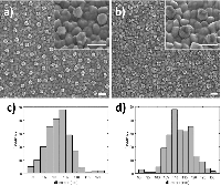
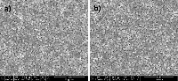
Deposition on bare ITO remains unchanged after pretreatment (Figure 5 black curves), but a large peak is observed around +50 mV in the cathodic half-wave of the first scan for gold disk-functionalized ITO (Figure 5, 1). The shift of the deposition peak back to a potential similar to that observed prior to pretreatment (Figure 3) suggests that the mechanism of this uniform deposition used here is dependant on the redox state of the outermost layer of the gold disks. The result of a 135-second deposition at –50 mV after pretreatment is seen in Figure 6.
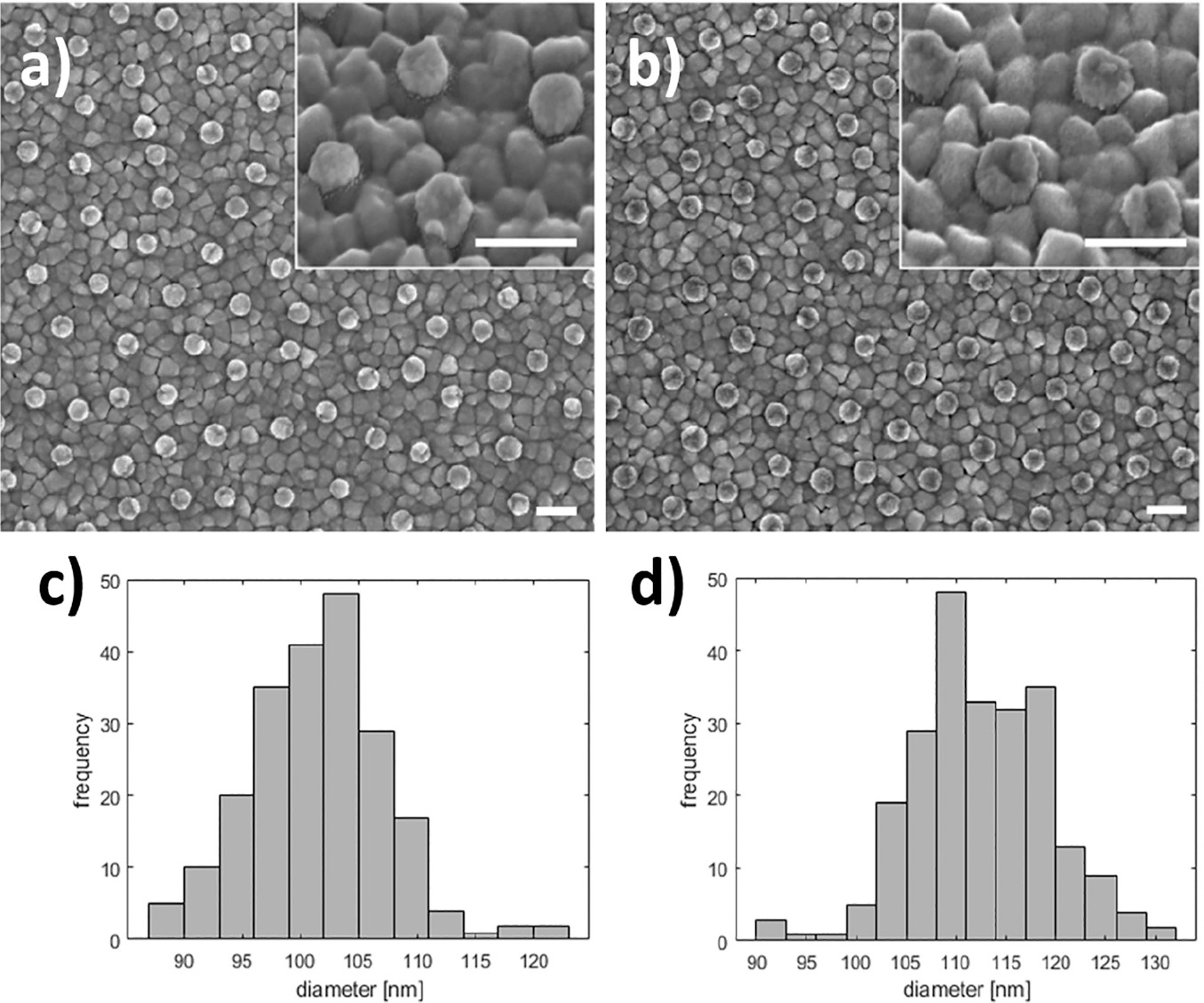
Figure 6 Silver deposition on pretreated gold nanodisks. SEM images show gold nanodisks on ITO before and after pretreatment and silver deposition (a and b, respectively) for 135 seconds at –50 mV in a deposition media containing 1 M NH3 and 500 μM AgNO3. Disk diameters were measured to 101.6±5.8 nm and 112.5±6.8 nm before and after deposition (c and d, respectively). Scale bars are 200 nm.
SEM analysis of before and after pretreatment and silver deposition show a uniform deposition of a roughly 5.5 nm thick layer of silver (Figure 6(a)–(d)).
Gold-catalyzed silver-enhancement of colloidal gold nanoparticles, driven by the redox potential of a reducing agent, has been used for well over thirty years as a means by which to enhance contrast of absorbed gold nanoparticles in immunoassays [28]. Although bulk gold is a poor catalyst, colloidal gold particles of sizes relevant for biological absorption show catalytic activity inversely proportional to size for a variety of reactions [29–31]. In ammonia, silver forms the complex Ag(NH3)2+, a compound known as Tollens’ reagent commonly used to determine presence of aldehydes by oxidizing the carbonyl group to carboxylate while reducing the complex silver ion to elemental silver through the following net reaction [32]:
\begin{equation} 2[\rm{Ag}(\rm{NH}_{3})_{2}]^{+} +\rm{RCHO}+\rm{H}_{2}O \rightarrow 2 \rm{Ag}(\rm{s}) + 4~\rm{NH}_{3}+\rm{RCO}_{2}\rm{H}+2~\rm{H}^{+} \end{equation}In a similar way, reduction of silver on gold nanoparticles might be stabilized by the introduction of surface oxides during pretreatment.
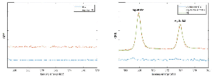
Preferential deposition of silver on the gold nanodisks was confirmed by X-ray photoelectron spectroscopy (XPS) analysis on bare ITO and gold nanodisks on ITO before and after silver deposition on the pretreated samples (Figure 7 and Figure S1). Silver was clearly observed on the nanodisk samples while no peaks corresponding to silver were detected on the ITO indicating that the level Ag deposited on bare ITO indicated by electrochemical methods (Figure 4(a)) are below the detection limit of XPS.
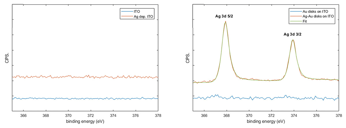
Figure 7 XPS data. Presence of silver was measured on bare ITO and nanodisk-functionalized ITO before and after pretreatment and silver deposition (a and b, repsectively).
Qualitative analysis of the growth mechanism was made by simultaneously recording the optical and amperometric response to silver deposition (Figure 8).
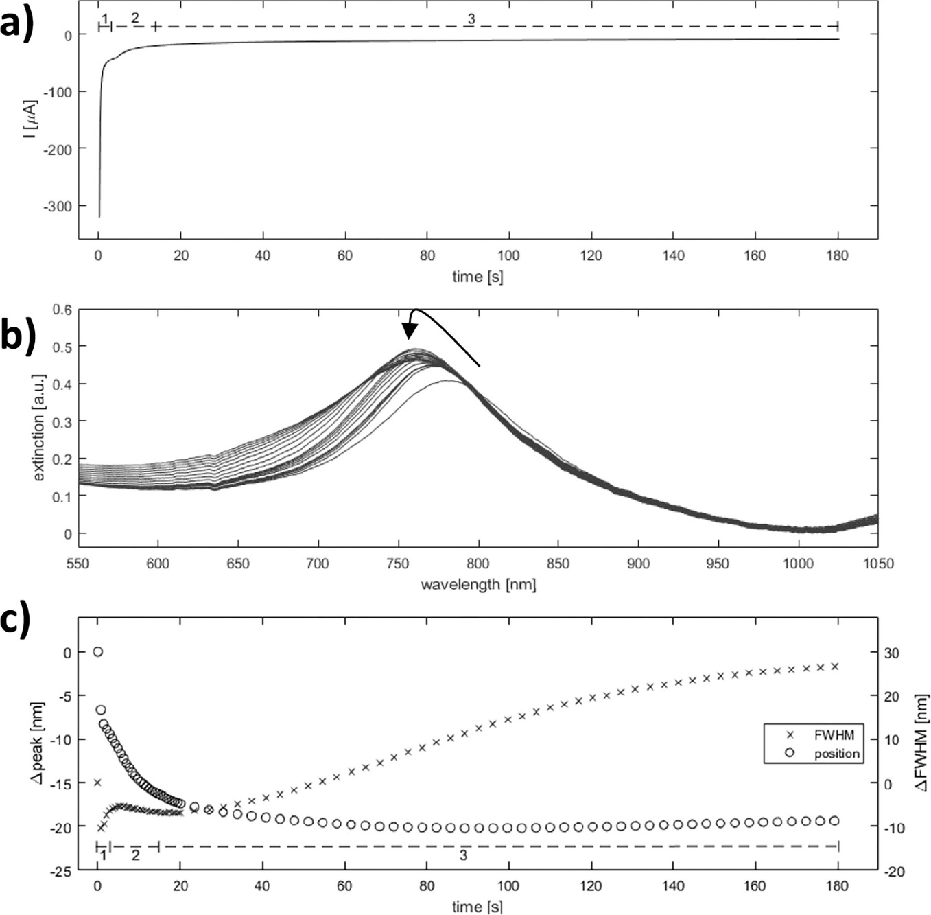
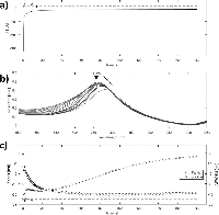
Figure 8 Spectroelectrochemical analysis of silver deposition on single disk system. Simultaneous optical and amperometric measurements were recorded during silver deposition on activated single-gold nanodisks. Approximate regions corresponding to double layer charging (1), oxide layer reduction (2), and diffusion controlled silver reduction (3) are shown in the chronoamperometric and quantized optical plots (a and c, respectively). The black arrow in the plot of raw optical spectra indicates evolution of peak (b).
The observed deposition curves indicate a complex process with three regimes at different times during deposition (regions 1, 2, and 3 in Figure 8(a) and (c)), which suggests up to three processes occurring. The large current spike at t=0 is due to capacitive charging of the electrode interface, decaying exponentially with time (Figure 8(a) region 1). The second region of the deposition curve is dominated by reduction of the outer oxide layer of the gold nanodisks, a surface controlled process, while the remaining part can be explained as diffusion-controlled reduction of silver (Figure 8(a) regions 2 and 3, respectively). Similar regions are recognized in the plot showing changes in peak position and FWHM of the plasmonic peak during deposition (Seen in Figure 8(b) and quantified in Figure 8(c)). Because of an increase of the electron density of the plasmonic structures, applying a negative potential (relative to OCP) blue-shifts the resonance peak [33, 34]. However, for the low potentials used here the effect is negligible, and the observed blue-shift is due mainly to reduction of the oxide layer covering the gold structures, reducing the refractive index and dampening of the resonance (Figure 8(c) region 1). The relatively rapid drop in peak width observed close to t=0 in Figure 8(c) is accompanied by a significant increase in peak height (Figure 8(b)). The drop appears as a transient effect, with a rapid increase again in FWHM, (Figure 8(c) region 1) in a background of a slower reduction of FWHM from the initial value (visible as region 2 in Figure 8(c)) and is suggested to be related to the rapidly changing capacitive current. General peak-broadening with slow variation of the resonance peak position is observed starting around 40 seconds into the deposition. This can be interpreted as inhomogenous or irregular growth of disk-diameter for longer deposition times, consistent with the observed broadening of the size distribution (Figure 6(c) and (d)).
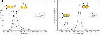
The same process was used with closely spaced gold disks. As the centre-to-centre distance between adjacent disks in a pair is dependent on the thickness of the hole-mask, and the disk diameter on the diameter of the polystyrene particles used in mask fabrication, a variation in disk spacing is expected due to substrate roughness and the polystyrene particle size distribution. Consistent results were obtained using fabrication parameters stated in the experimental section and with a deposition time of 135 seconds at –50 mV in a 1 M NH3 solution containing 500 μM AgNO3 (Figure 9).
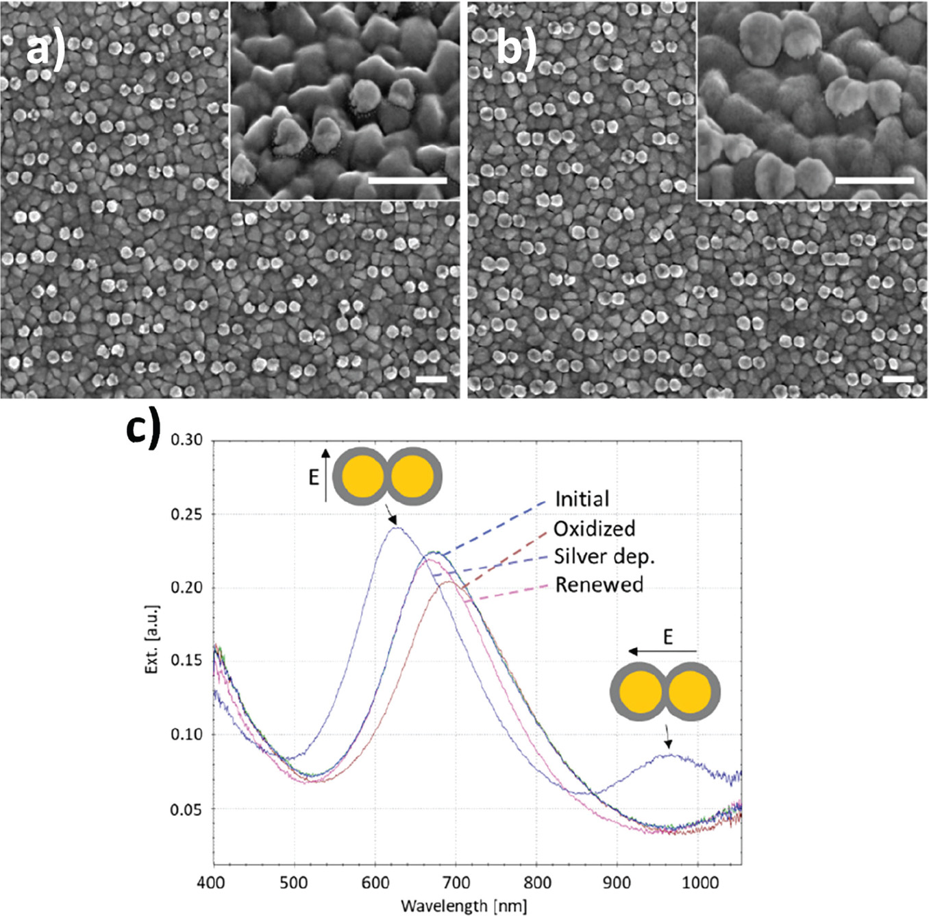
Figure 9 Silver deposition on gold nanodisk pairs. SEM images show disk pairs before (a) and after (b) pretreatment and silver deposition for 135 seconds at –50 mV in a deposition media containing 1 M NH3 and 500 μM AgNO3. c), optical spectra recorded at each step in the deposition process. Surface oxide formation during the activation step causes a red-shift of the resonance peak (brown trace). Arrows indicate position of transverse and longitudinal modes, respectively. Spectral shape after renewal returns to that of the initial non-connected sample (pink and blue traces, respectively).
A relatively low yield of connected pairs of 19.5% after deposition (versus 2.41% before deposition) was a consequence of a fabrication compromise between disk spacing and pre-deposition connected disk pairs (Figure 9(a) and (b)). Figure 9(c) shows the optical spectra recorded at each step in the deposition process. The peak shape for the clean, unconnected disk pairs shows asymmetry similar to that observed in Figure 2(c), consistent with plasmon hybridisation theory (blue curve, Figure 9(c)). Growth of gold oxides on the structures during oxidation in preparation for silver deposition causes a red-shift and lowering of intensity of the optical spectrum, due to a damping effect of the oxide layer (brown curve, Figure 9(c)). After silver deposition blue-shift of the main resonance peak as well as appearance of a secondary peak in the NIR region is observed (arrows, Figure 9(c)). The position of these features correspond well with FDTD simulations with parameters obtained from the SEM images in Figure 6(b) and Figure 9(a) and (b) (Figure 10(b)). The surface was renewed by removal of silver in a stirred solution containing 1 M NH3 applying 10 cycles of cyclic voltammetry between –50 mV and 400 mV at a scan rate of 50 mV/s. This returned the optical spectrum to that of the initial sample (Figure 9(c), pink trace).
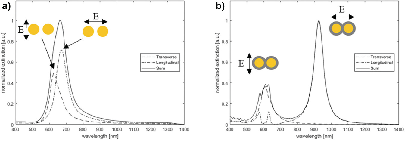
Figure 10 FDTD simulations.
Simulations on non-connected disk pairs show the expected splitting of peaks through hybridisation with the lower-energy coupling mode for longitudinally polarized light and higher energy coupled mode for the transversely polarized light, resulting in an asymmetric peak shape for the summed spectra (Figure 10(a)). The proportionality discrepancy observed between simulation and measured data (Figure 9(c), initial) is due to the simulation model not including variation in disk diameter in each disk pair and spacing. For connected pairs, the simulation is able to predict the spectral position of the longitudinal dipole mode with reasonable accuracy (925 nm versus 962 nm measured). The significantly lower low energy peak in the experimental data fits with the observation from the SEM images that the majority of the pairs do not become connected. As before, neither dimensional variation nor low yield of connected pairs are accounted for.
4 Conclusion
In this work we have demonstrated a method for quasi-reversible switching of the longitudinal dipole mode in pairs of closely spaced gold nanodisks to induce a resonance at a specified wavelength (here in the near infrared). The use of different disk diameters could allow this spectral position to be selected. While a relatively low yield of connected pairs after silver deposition was observed, caused by roughness of the ITO surface and the polydispersity of the colloidal particles, both these can be improved by using lower-roughness substrates (i.e. zinc-doped indium oxide [35]) and lower-dispersity polystyrene particles during hole-mask fabrication, which would enable both closer and more uniform spacing of disks in pairs. Such active plasmonic elements prepared over large area can have use as optical switching devices.
Acknowledgements
The European Commission H2020 grant (Symbiotic 665046 project) is acknowledged for the funding that made this work possible.
Supplementary
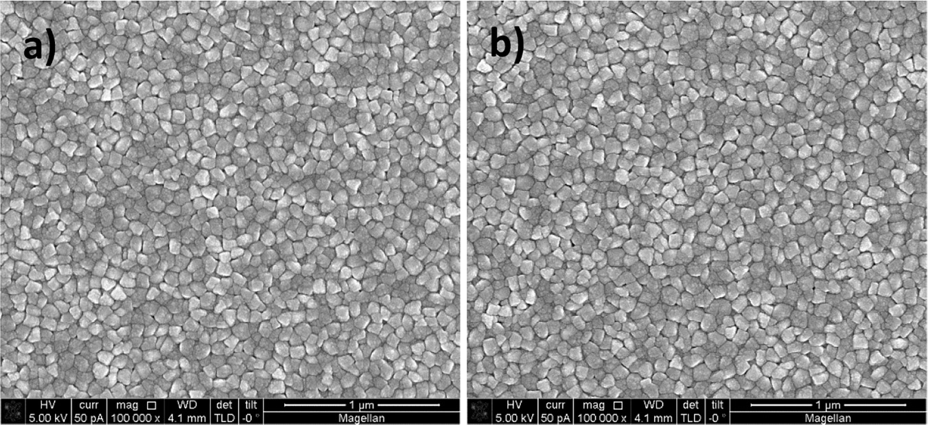
Figure S1 SEM images show ITO before and after pretreatment and silver deposition (a and b, respectively) for 135 seconds at –50 mV in a deposition media containing 1 M NH3 and 500 μM AgNO3.
References
[1] E. de Harven, R. Leung, and H. Christensen, “A novel approach for scanning electron microscopy of colloidal gold-labeled cell surfaces.,” J. Cell Biol., vol. 99, no. 1 Pt 1, pp. 53–7, Jul. 1984.
[2] L. Seopsi, L.-I. Larsson, L. Bastholm, and M. H. Nielsen, “Silver-enhanced colloidal gold probes as markers for scanning electron microscopy,” Histochemistry, vol. 86, no. 1, pp. 35–41, 1986.
[3] I. H. El-Sayed, X. Huang, and M. A. El-Sayed, “Surface Plasmon Resonance Scattering and Absorption of anti-EGFR Antibody Conjugated Gold Nanoparticles in Cancer Diagnostics: Applications in Oral Cancer,” 2005.
[4] T. Gong, D. Goh, M. Olivo, and K.-T. Yong, “In vitro toxicity and bioimaging studies of gold nanorods formulations coated with biofunctional thiol-PEG molecules and Pluronic block copolymers,” Beilstein J. Nanotechnol, vol. 5, pp. 546–553, 2014.
[5] P. Ciaurriz, F. FernC!ndez, E. Tellechea, J. F. Moran, and A. C. Asensio, “Comparison of four functionalization methods of gold nanoparticles for enhancing the enzyme-linked immunosorbent assay (ELISA).,” Beilstein J. Nanotechnol., vol. 8, pp. 244–253, 2017.
[6] J. Su, Z. Zhou, H. Li, and S. Liu, “Quantitative detection of human chorionic gonadotropin antigen via immunogold chromatographic test strips,” 2014.
[7] S. V. Boriskina and B. M. Reinhard, “Molding the flow of light on the nanoscale: from vortex nanogears to phase-operated plasmonic machinery,” Nanoscale, vol. 4, no. 1, pp. 76–90, Dec. 2012.
[8] E. Hutter and J. H. Fendler, “Exploitation of localized surface plasmon resonance,” Adv. Mater., vol. 16, no. 19, pp. 1685–1706, 2004.
[9] E. M. Larsson, J. Alegret, M. Ka, and D. S. Sutherland, “Sensing Characteristics of NIR Localized Surface Plasmon Resonances in Gold Nanorings for Application as Ultrasensitive Biosensors,” 2007.
[10] “The investigation of an LSPR refractive index sensor based on periodic gold nanorings array,” 2018.
[11] M. Li, S. K. Cushing, and N. Wu, “Plasmon-Enhanced Optical Sensors: A Review.”
[12] M. Kang, J.-J. Kim, Y.-J. Oh, S.-G. Park, and K.-H. Jeong, “A Deformable Nanoplasmonic Membrane Reveals Universal Correlations Between Plasmon Resonance and Surface Enhanced Raman Scattering,” Adv. Mater., vol. 26, no. 26, pp. 4510–4514, Jul. 2014.
[13] C. P. Byers et al., “From tunable core-shell nanoparticles to plasmonic drawbridges: Active control of nanoparticle optical properties,” Sci. Adv., vol. 1, no. 11, pp. e1500988–e1500988, Dec. 2015.
[14] M. Chirea, S. S. E. Collins, X. Wei, and P. Mulvaney, “Spectroelectrochemistry of Silver Deposition on Single Gold Nanocrystals,” J. Phys. Chem. Lett, vol. 5, p. 35, 2014.
[15] M. Frederiksen and D. S. Sutherland, “Direct modification of colloidal hole-masks for locally ordered hetero-assemblies of nanostructures over large areas,” Nanoscale, vol. 6, no. 2, pp. 731–735, Dec. 2014.
[16] P. B. Johnson and R. W. Christy, “Optical Constants of the Noble Metals,” Phys. Rev. B, vol. 6, no. 12, pp. 4370–4379, Dec. 1972.
[17] T. A. F. KC6nig et al., “Electrically Tunable Plasmonic Behavior of Nanocube–Polymer Nanomaterials Induced by a Redox-Active Electrochromic Polymer,” ACS Nano, vol. 8, no. 6, pp. 6182–6192, Jun. 2014.
[18] J. Cao, T. Sun, and K. T. V. Grattan, “Gold nanorod-based localized surface plasmon resonance biosensors: A review,” Sensors Actuators B Chem., vol. 195, pp. 332–351, May 2014.
[19] E. Prodan, C. Radloff, N. J. Halas, and P. Nordlander, “A Hybridization Model for the Plasmon Response of Complex Nanostructures,” Science (80-.)., vol. 302, no. 5644, pp. 419–422, Oct. 2003.
[20] * Per Hanarp, and Mikael Käll, and D. S. Sutherland, “Optical Properties of Short Range Ordered Arrays of Nanometer Gold Disks Prepared by Colloidal Lithography,” 2003.
[21] P. Nordlander, C. Oubre, E. Prodan, K. Li, and M. I. Stockman, “Plasmon Hybridization in Nanoparticle Dimers,” vol. 14, p. 44, 2018.
[22] V. Myroshnychenko et al., “Modelling the optical response of gold nanoparticles,” Chem. Soc. Rev., vol. 37, no. 9, p. 1792, Aug. 2008.
[23] N. Zohar, L. Chuntonov, and G. Haran, “The simplest plasmonic molecules: Metal nanoparticle dimers and trimers,” J. Photochem. Photobiol. C Photochem. Rev., vol. 21, pp. 26–39, 2014.
[24] D. Zhang and Y. Tang, “Enhancing light reflective properties on ITO glass by plasmonic effect of silver nanoparticles,” Results Phys., vol. 7, pp. 2874–2877, Jan. 2017.
[25] Y. Feng et al., “Uniform Large-Area Free-Standing Silver Nanowire Arrays on Transparent Conducting Substrates,” J. Electrochem. Soc., vol. 163, no. 8, pp. D447–D452, Jun. 2016.
[26] R. Sivasubramanian and M. V. Sangaranarayanan, “A facile formation of silver dendrites on indium tin oxide surfaces using electrodeposition and amperometric sensing of hydrazine,” Sensors Actuators B Chem., vol. 213, pp. 92–101, Jul. 2015.
[27] D. Hernández-Santos, M. González-García, and A. Costa-García, “Electrochemical determination of gold nanoparticles in colloidal solutions,” Electrochim. Acta, vol. 46, no. 4, pp. 607–615, Dec. 2000.
[28] C. S. Holgate, P. Jackson, P. N. Cowen, and C. C. Bird, “The Journal of Histochemistry and Cytochemistry Immunogold-Silver Staining: New Method of Immunostaining with Enhanced Sensitivity’,” 1983.
[29] A. Corma and H. Garcia, “Supported gold nanoparticles as catalysts for organic reactionsw,” 2008.
[30] D. V Jawale et al., “Size effect of gold nanoparticles supported on carbon nanotube as catalysts in selected organic reactions,” Tetrahedron, vol. 70, pp. 6140–6145, 2014.
[31] P. Suchomel et al., “Simple size-controlled synthesis of Au nanoparticles and their size-dependent catalytic activity OPEN.”
[32] W. E. Benet, G. S. Lewis, L. Z. Yang, and P. D. E. Hughes, “The mechanism of the reaction of the Tollens reagent,” J. Chem. Res., vol. 35, no. 12, pp. 675–677, Dec. 2011.
[33] T. Ung, M. Giersig, D. Dunstan, and P. Mulvaney, “Spectroelectrochemistry of Colloidal Silver,” 1997.
[34] A. B. Dahlin et al., “Electrochemical plasmonic sensors,” Anal. Bioanal. Chem., vol. 402, no. 5, pp. 1773–1784, Feb. 2012.
[35] G. GonC'alves, E. Elangovan, P. Barquinha, L. Pereira, R. Martins, and E. Fortunato, “Influence of post-annealing temperature on the properties exhibited by ITO, IZO and GZO thin films,” Thin Solid Films, vol. 515, no. 24, pp. 8562–8566, Oct. 2007.
Biographies

Hans Dyrnesli (Ph.D. student) received his M.Sc. in Molecular Biology in 2015 from the University of Aarhus, Denmark, under the supervision of Associate Professor Kenneth A. Howard, and is completing his Ph.D. studies in Nanoscience in 2019 at the Interdisciplinary Nanoscience Center (iNANO), Aarhus University, Denmark under the supervision of Professor Duncan S. Sutherland.

Gunnar Klös, currently Ph.D. student in Professor Duncan S. Sutherland's group at the iNANO department of Aarhus University, obtained his BSc degree in physics in 2013 from the Georg-August University GC6ttingen, where he also obtained his MSc degree in 2015, specialising in the Physcis of Complex Systems at the MPI for Dynamics and Self-Organization. His research interest are chiral plasmonic nano-structures for biosensor applications, using large-area lithographic techniques and electromagnetic simulations.
Matteo Miola (Ph.D. student) received his M.Sc. (2015) in Material Science and Engineering from the University of Padova. He is completing his Ph.D. studies (2019) in the carbon dioxide activation center (CADIAC) at Aarhus University on the heterogeneous electrochemical carbon dioxide reduction under the supervision of Professor Kim Daasbjerg.

Duncan S. Sutherland (Professor) received his Ph.D. in 1995 in Physics in the area of Biomaterials surface science from the University of Bristol. He spent 10.5 years at the Dept of Applied Physics Chalmers Sweden before moving his group to the iNANO center at Aarhus University in 2006. His research interests are in the areas of nanoscale phenomena at biointerfaces, nanofabrication and nanooptics in the context of biosensors, molecular cell biology and nanoparticle toxicology.