Methods of Synthesis and Characterization of Conductive DNA Nanowires Based on Metal Ion-Mediated Base Pairing for Single-Molecule Electronics
Simon Vecchioni1, Mark C. Capece2, Emily Toomey3, Lynn Rothschild4 and Shalom J.Wind5
1Department of Biomedical Engineering at Columbia University, New York, NY 10027, USA
2Department of Chemistry, Stanford University, Stanford, CA 94305, USA
3Department of Electrical Engineering and Computer Science, Massachusetts Institute of Technology, Cambridge, MA 02139, USA
4NASA Ames Research Center, Space Science and Astrobiology Division, Moffett Field, CA 94035, USA
5Department of Applied Physics and Applied Mathematics at Columbia University, New York, NY 10027, USA
E-mail: sw2128@columbia.edu
Received 29 August 2018; Accepted 27 December 2018;
Publication 31 January 2019
Abstract
Advances in the field of molecular electronics have made possible the direct measurement of charge transport across single molecules. In particular, work on DNA oligomers has demonstrated that this weakly-conducting biomolecule can be functionalized through metal-mediated nucleobase pairing in order to significantly increase electron mobility across the molecule. The introduction of interacting stacks of single metal ions inside the DNA helix is an attractive platform for assay and optimization; for this reason we present a protocol for the production and processing of nanowires with a metal base pair for single-molecule applications. In particular, we describe the construction of DNA duplex wires with a cytosine-Ag+-cytosine base pair (dC:Ag+:dC). A thorough investigation of buffer components suggests the use of divalent magnesium counterions to stabilize highly mismatched oligonucleotides in solution. We further analyse cleaning and processing of thin gold films for batch-fabrication of conductive imaging substrates for use in conductive scanning probe assays of single-molecule conductivity. With a clear path to electrical assays, we suggest that the C:Ag+:C orthogonal nucleotide pair and other similar chemistries may provide a foundation for molecular electronic components in integrated devices.
Keywords
- Molecular electronics
- DNA nanowire
- nanomaterials
- cytosine mismatch
- methods
1 Introduction
The study of electrical conductivity in DNA has produced a diversity of results which have been largely influenced by experimental design. Early studies on viral DNA demonstrated resistive behavior [1], while microbial DNA was suggested to have an RFID-like signal in bulk solution [2]. Subsequent attempts to probe the current carrying properties of DNA have followed many approaches with a variety of results: small bundles of DNA have shown high insulation [3]; cooled DNA displayed induced super-conductivity [4]; cAFM across guanine tetraplexes has demonstrated semiconducting behaviour [5]; and, recently, scanning tunneling microscope (STM) studies have reliably shown weak conductivity in stacked dG:dC pairs [6].
The atomic scale break junction platform, based on the scanning tunneling microscope, has become a mainstay of the field of molecular electronics, and it has proven to be a reliable and reproducible method for the assay of electron tunneling across single molecules [7, 8]. This result relies upon a reversible covalent linkage between a gold STM tip and one end of a molecule in tandem with a linkage between the other end of the molecule and a metal – generally an atomically-flat gold substrate. By oscillating the tip elevation in order to form and break contact with single molecules, it is possible to measure charge transfer across the molecule in the presence of a voltage bias and to construct height-dependent current plots that represent the ability of electrons to tunnel across the gap, that is, through the molecule itself. Because this can be repeated rapidly – up to thousands of times within a short measurement period – statistical methods can be applied to determine the minimal step size between measured currents, thereby allowing a determination of the resistance of the molecule itself. This has proven a powerful method for the study of conductance in molecules in units of the quantum conductance, since each measurement can be calibrated to a gold-to-gold atomic junction. This technique has shown repeatable differences in conductance between DNA molecules of different lengths [9] and sequence composition [6], and, recently, a significant difference between the electrical behavior of canonical Watson-Crick strands and DNA duplexes with orthogonal binding chemistry [10].
With experimental evidence that charge transport in native DNA decays over any meaningful distance [1, 9], efforts have focused on approaches to increase DNA conductance by design. In particular, the development of metal binding schemes either through ion-coordinating pyrimidine-mismatch systems [11–13], or proposed schemes built on orthogonal nucleobases [14, 15], have generated a great deal of interest in the role of electrically-functional nucleic acid nanotechnology. It has long been hypothesized that the discovery of metal-mediated base pairs would allow for the construction of electrically-active DNA elements, but the lack of molecular resolution in conductivity assays made it difficult to study these systems. Until recently, chemical and thermodynamic characterization of orthogonal DNA chemistries prevailed. Structural studies on these systems [16, 17] and improved tight-binding (TB) and density functional theory (DFT) simulations of canonical DNA [18, 19] suggested that the reduction of inter-pair distances, the hopping of electrons along bases with similar energy levels, and the depletion of dA:dT pairs could improve results in electron mobility. A key study showing the electrical functionality of guanine tetraplexes opened the door to direct electrical studies in altered-chemistry nucleic acids [5].
Building upon advances in metal-mediated pairing [11, 20], we insert silver (Ag+) ions into the helical gaps between mismatched cytosine bases to form molecular wires using the C-Ag+-C base pair (Figure 1). Using the well-defined STM break junction technique, we recently described enhanced conductivity in Ag+-paired polycytosine oligomers versus canonically-paired analogs [10]. Here we describe the exact protocols and binding chemistries for construction of these molecules for use in STM and other electrode-based single molecule conductivity studies.
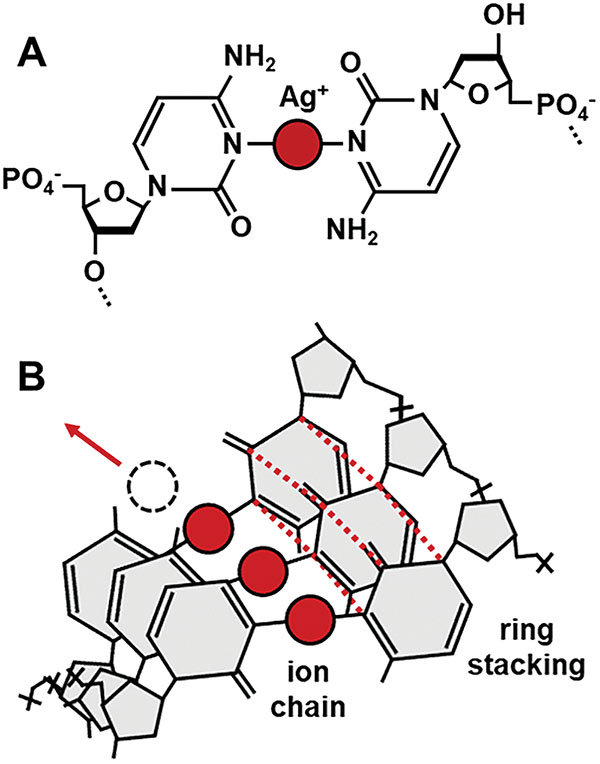
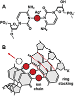
Figure 1 Bond and ion coordination chain. A) The C:Ag+:C base pair coordinates a silver ion between opposing nitrogen atoms (N3 ring position). B) Homobase oligomers exhibit stacking of coordinated rings; while stacked ion-pairs are expected to exhibit metallophilic compression through interactions between the ions [13], which suggests a novel conduction pathway.
2 Materials
In order to prepare Ag+-mediated DNA nanowires in solution, the following equipment and reagents are required:
- DNA preparation reagents
- Polyacrylamide gel electrophoresis (PAGE)-purified oligonucleotides with appropriate linking chemistry (see text for details, Section 3.1)
- Nuclease-free (molecular biology grade) deionized water (Thermo Fisher Scientific, Waltham, MA, #4387936); or diethylpyrocarbonate-treated (DEPC) water (Thermo Fisher, #AM9922) if utilizing downstream RNA application
- MOPS (3-(N-morpholino)propanesulfonic acid)
- Sodium nitrate
- Silver nitrate
- Sodium chloride
- Magnesium sulfate heptahydrate (Epsom salt) or other non-chlorinated magnesium salt
- 10% Sulfuric acid (diluted from stock in nuclease-free water)
- 10% Sodium hydroxide (diluted from stock in nuclease-free water)
- DNA preparation equipment (all sterile and nuclease free)
- Falcon tubes (15 mL)
- Micro-centrifuge (microfuge) tubes (1 mL)
- Microfuge tubes (100 μL)
- Pipettes (1 mL, 100 μL, <20 μL sizes)
- Pipette tips
- Parafilm
- Scale and weigh boats or equivalent
- Hot block with temperature control up to 100∘C or water bath (Styrofoam box and 2 L beaker of water can suffice)
- Tabletop centrifuge
- Vortex mixer
In order to prepare atomically-flat gold substrates for imaging, the following equipment and reagents are required:
- Gold surface preparation reagents
- Hydrogen peroxide (H2O2) 30% (e.g., H325-500, Thermo Fisher Scientific, Waltham, MA, USA)
- Sulfuric acid (H2SO4) ∼36 Normal (e.g., A300-500, Fisher)
- Deionized water
- Ethanol (95%)
- Gold surface preparation equipment
- Silicon (100) wafer with 300 nm, undoped, N-type silicon dioxide layer, 3 in x 0.50 mm (e.g., SI-SO-Ua76D05C1-300nm, MTI Corporation, Richmond, CA, USA)
- Non-reactive metal tweezers (e.g., 533, Ted Pella Inc., Redding, CA, USA)
- 3 x 90 mm glass plates with lids (wafer sized)
- Conductive liquid silver paint (e.g., 16034, Ted Pella)
- Cleanroom-based electron beam evaporation chamber with gold pocket (e.g., Angstrom EvoVac, Angstrom Scientific, Ramsey, NJ, USA)
- Oxygen plasma cleaner, tabletop model (e.g., 18W PDC-32G, Harrick Plasma Inc., Ithaca, NY, USA)
- Annealing furnace or CVD chamber with forming gas (Ar/H2) environment
3 Choosing a System: DNA Preparation
3.1 DNA Functionalization
The sample sequence used in this work is an 11 nucleotide (nt) polycytosine which can either form a silver-coordinating duplex with 11 Ag+ ions and two C11 oligos, or a native duplex with C11 and its Watson-Crick reverse complementary sequence, G11 (Table 1). This sequence is selected because it provides an excellent template and is the basis of previous molecular electronics work [10]. While polycytosine oligomers suffer badly from alignment issues during annealing, the C11 oligo is short enough that it preferentially forms a duplex without an overhang [21]. Longer polycytosines begin to form sticky-end-like duplexes that anneal into long chains—also interesting as electrical wires, but their length and inhomogeneity makes them unsuitable for straightforward electrical characterization. Furthermore, the C11 molecule demonstrates a very high thermal stability and shows a lack of nanocluster formation after annealing with Ag+ (unpublished data).
Table 1 Oligonucleotide sequences
| Code | Sequence Name | Sequence with IDT DNA Mod Codes |
| [1A] | C11 thiol | CCC CCC CCC CC /3ThioMC3-D/ |
| [1B] | G11 thiol | GGG GGG GGG GG /3ThioMC3-D/ |
| [2A] | C11 amine | /5AmMC6/ CCC CCC CCC CC |
| [2B] | G11 amine | /5AmMC6/ GGG GGG GGG GG |
| [3A] | C11 overhang | CCC CCC CCC CCA |
| [3B] | G11 overhang | GGG GGG GGG GGA |
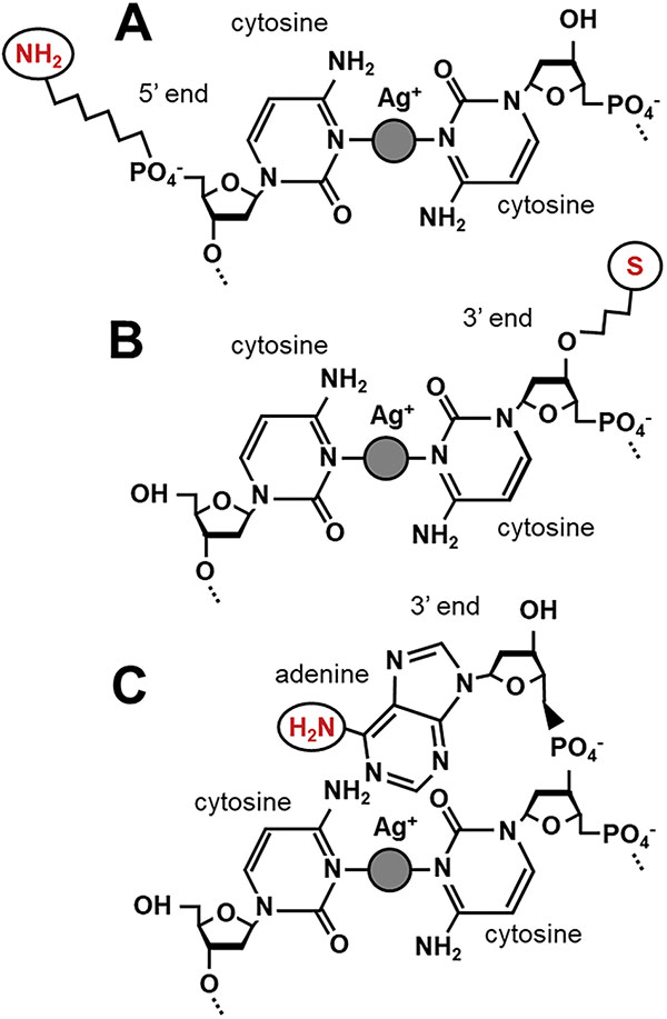
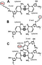
Figure 2 Linker chemistries. A) 5′ C6 amine provides a stable link with higher resistance. B) 3′ C3 thiol provides a more volatile link with lower resistance. C) Overhanging terminal adenines present primary amines that can be used to directly access the DNA ring structure.
In order to perform direct electrical measurements or other operations on DNA duplexes, a chemical linker must be used to access the ring system or ion coordination chain inside the double helix (Figure 2). Every linker system has its advantages, but none offers the perfect electrical contact. Amines provide weaker coupling than thiols and are known to chelate silver ions, while thiols are unstable electrically and add noise into the measurement [22]. To reduce the effects of chelation on bond availability, Ag+ not coordinating cytosine mismatches is precipitated out as AgCl (Figure 3). Standard linkers that are obtained commercially often come with three- or six-carbon spacers (C3, C6) between the DNA oligo and the functional group, providing steric accessibility but generating a good deal of contact resistance and reducing the measured conductivity of the molecule (see [6] vs. [9]). Commercially available linkers are furthermore added to the phosphate backbone of these molecules and are consequently in direct contact with the least conductive part of the DNA molecule. Here we describe a single nucleobase overhang in which the native C6-site amine of adenine is used as a substitute for longer linkers. This allows an electrical contact directly into the ring system of the DNA and is at most 4–6 Å from the ion chain in a terminal dC:Ag+:dC bond.
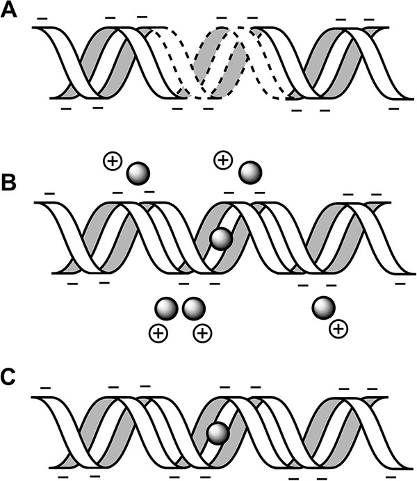
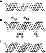
Figure 3 Duplex annealing and ion localization. A) DNA strand with mismatches in the absence of Ag+. B) After annealing with Ag+, ions are coordinated between cytosine mismatches and also form weaker electrostatic interactions with phosphate groups on the backbone. C) Precipitation of AgCl does not perturb cytosine-coordinated ions but does strip Ag+ from the backbone.
The DNA oligos themselves can be ordered from a variety of commercial sources, such as Integrated DNA Technologies (IDT, Coralville, IA, USA) or Elim Biopharmceuticals (Hayward, CA, USA). For convenience, the modification codes for IDT ordering are added to sequences in Table 1. To ensure the purity of the oligonucleotides and exclude any outlying sequences, the strands should be either PAGE- and/or high-performance liquid chromatography (HPLC)-purified. Some companies such as IDT ship their DNA dry, which allows for a longer shelf life. If shipped in deionized water, it would be wise to check the concentration and either correct to 100 μM or adjust the protocol accordingly (see Table 2 recipes). If shipped dry, add nuclease-free water and pipette vigorously to ensure DNA is fully resuspended. A final concentration of 100 μM corresponds to 10 μL per nmol of oligonucleotide.
3.2 Selecting a Buffer
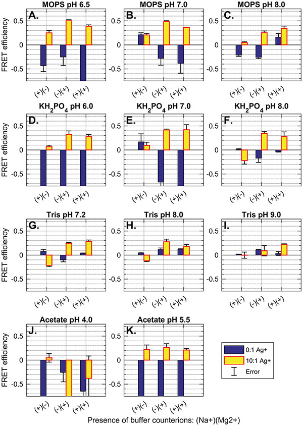
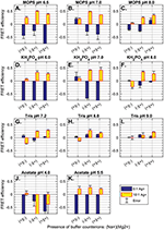
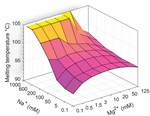
Figure 4 Comparison of FRET efficiency (normalized fluorescence quenching) of palindromic 30 nt polycytosine “C30”—5′-FAM-CCCCCCCCCCCCCCCCCCCCCCCCCCCCCC-BHQ1-3′ in buffers with varying buffer salts, counterions, pH and Ag+ availability. Buffer and pH are indicated in plot titles. Counterion species are indicated on the X-axes, where (+)(-) denotes 100 mM Na+; (-)(+) denotes 12.5 mM Mg2+, and (+)(+) indicates 100 mM Na+ and 12.5 mM Mg2+. Error bars show standard deviation for FRET efficiency (n = 3). Presence of 0:1 Ag+ molarity compared to sequence mismatches (blue) and 10:1 Ag+ molarity to sequence mismatches (yellow) is indicated by bar color (see legend). Complete buffer recipes can be found in the supplemental information (Tables S1-S2). For both MOPS buffers and potassium phosphate buffers, the presence of Mg2+ greatly increases FRET efficiency and strand annealing: A) MOPS pH 6.5, B) MOPS pH 7.0, C) MOPS pH 8.0; and D) KH2PO4 pH 6.0, E) KH2PO4 pH 7.0, F) KH2PO4 pH 8.0. The same trend is observed for Tris buffers, but with greatly reduced efficiency throughout: G) Tris pH 7.2, H) Tris 8.0, and I) Tris 9.0. Low pH sodium acetate buffer does not promote duplex formation: J) NaAc pH 4.0; while higher pH acetate buffer promotes i-motif formation across all counterion conditions: K) NaAc pH 5.5. This conclusion is supported by the lack of FRET quenching in control strand AT24 in similar buffer (Figure S1). In all buffers, acidic pH (≤ pH 7.0) promotes fluorescence enhancement (negative FRET efficiency) after annealing, while basic pH (> pH 7.0) dampened the fluorescence signal overall, both fluorescence and quenching.
3.2.1 General considerations: Ag+ compatibility
The choice of buffer will determine the favorability of ion uptake. For the most part, standard annealing buffers are appropriate for Ag+-functionalized DNA nanowires [20], with several caveats. Most importantly, there should be minimal presence of chloride ions, as silver chloride is highly insoluble. At high temperature, 1H-1H COSY NMR suggests that cytosine-mismatched oligonucleotides can outcompete anions for Ag+ when already incorporated into the DNA (manuscript in preparation), but it is best to avoid the confounding effect of precipitation. This means that the researcher should avoid adjusting buffer pH with HCl, as this can leave residual Cl- of relatively high molarity. Furthermore, there should be no chelating buffer agents. Thus, ethylenediaminetetraacetic acid (EDTA) and other Mg2+ intercalators should be avoided, rendering buffers such as Tris-acetate-EDTA (TAE) and Tris-borate-EDTA (TBE) inappropriate for annealing. These buffers are still acceptable for downstream applications such as gel electrophoresis after Ag+ is already snugly bound by a cytosine-mismatched duplex.
Several other considerations are less obvious. To elucidate the effects of buffer component species, we screened 33 buffers with different buffer salt, pH, counterion species and Ag+ availability. The experiment was performed by mixing MOPS, potassium phosphate, Tris, and sodium acetate buffers at standard reaction concentrations (see Supplementary Tables 1–2) with either 100 mM Na+, 12.5 mM Mg2+, or both counterions. Oligonucleotides C30 (5′-FAM-CCCCCCCCCCCCCCCCCCCCCCCCCCCCCC-BHQ1-3′) and AT24 (5′FAM-AACAATACATACTAAAACCAAAAT-BHQ1-3′, 5′-ATTTTGGTTTTAGTATGTATTGTT-BHQ1-3′) (Elim Biopharmaceuticals) were labeled with 5′ fluorescein (FAM) and 3′ Black Hole Quencher 1 (BHQ1), which, when in close proximity, will cause Förster resonance energy transfer (FRET), whereby BHQ1 will absorb and suppress the signal from FAM, to cause an overall quenching in the fluorescence. Data were collected by measuring fluorescence before and after annealing of labeled oligos (2 μM per strand, or 4 μM for palindromic C30), either with or without 10x Ag+(600 μM). FRET efficiency was calculated by normalizing to the minimum FRET efficiency in deionized water, and the maximum efficiency (100% quenching). FRET is never 100% due to the promiscuity of the C30 sequence—it may anneal out of frame to form a daisy-chain type structure and thus prevent full quenching by annealed duplexes. The results can be seen in Figure 4.
3.2.2 Counterion species: Na+ and Mg2+
Thermodynamic simulations implemented in Matlab based on the best-available nearest neighbor and buffer correction models [24, 25] suggest that in Watson-Crick pairing sequences, [C30:G30] will have weak stabilization by Mg2+, but will experience a strong increase in thermostability due to Na+ association with the phosphosugar backbone (Figure 5). The presence of both counterions should have an intermediary effect, increasing the melting temperature and subsequent strength of duplexing relative to deionized conditions, but to a lesser degree than Na+ alone. Control sequence AT24 is predicted by a similar analysis to be stabilized equally by buffers containing Na+, Mg2+, or both. Experimentally we find results for C30, when stabilized by Ag+, that are not in agreement with this model, suggesting that the binding mechanism does not adhere to traditional Watson-Crick thermodynamics. To account for these differences, future studies may inform a more accurate thermodynamic model to accommodate orthogonal ion pairing. Preliminary insight on how to do this is provided by Torigoe et al. [11], but more work is needed to match the level of analysis available for canonical base pairs.

Figure 5 Thermodynamic simulation of buffer counterion effects on [C30:G30]. Nearest neighbor models based on Peyret et al. [24] and buffer correction equations from Owczarzy et al. at IDT DNA [25] allow for melting temperature modelling of oligonucleotides based on sequence and buffer composition. We implement these methods in Matlab to investigate the predicted effects of Na+ and Mg2+ on the thermostability of Watson Crick pairing of C30 (5′-CCCCCCCCCCCCCCCCCCCCCCCCCCCCCC-3′) to G30 (5′-GGGGGGGGGGGGGGGGGGGGGGGGGGGGGG-3′). The canonical model suggests a strong stabilizing effect by Na+, but little to no contribution by Mg2+. Experimental data on ion paired C30 suggests that the opposite is true, and that a new computational model is needed to account for orthogonal metal pairs.
In intermediary-pH MOPS and phosphate buffers, the C30 sequence demonstrates minimal fluorescence quenching in the presence of monovalent cation Na+ alone (Figure 4 A–F). The addition of Mg2+ causes maximal FRET efficiency of ∼0.5. The presence of both Na+ and Mg2+ together still promotes FRET, but in no case does the combined counterion solution outperform the buffer containing only divalent cations by any statistically significant amount. There are two potential reasons for the success of Mg2+ buffers. It may be the case that axial compression due to metallophilic attraction between stacked silver ions may cause crowding effects on monovalent counterions such as Na+, creating a need for the higher charge density offered by divalent cations such as Mg2+ in order to stabilize duplex formation in highly-cytosinated oligos. It may also be the case that divalent cations are better at sterically hindering Ag+ during the annealing process, causing intermediary, misaligned states to have a lower energy availability. This may force strand rearrangement to better-aligned duplexes which exhibit a higher degree of FRET quenching due to the better terminal fluorophore-quencher proximity. In either case, it is clear that Mg2+ provides a significant boost to FRET efficiency, and thus to duplex formation in cytosine-mismatched nanowires.
3.2.3 Buffer pH
It is known that buffer pH at or below 6.5 promotes the formation of cytosine-quadruplex (i-motif) DNA in the presence of oligos with high cytosine counts [26]. This structure forms non-B-form DNA that, to our knowledge, has not been assayed for electrical conductivity. Experimentation on this effect shows that low pH sodium acetate (pH 4.0) inhibits formation of any coherent structure (Figure 4J). Evidence of i-motif formation can be seen in medium-acidity acetate buffer (Figure 4K) by the observation of successful quenching only in excess Ag+ as well as a general insensitivity to counterion species. By contrast, AT24 does not cause FRET quenching either with or without Ag+, highlighting the requirement of cytosine bases in formation of acid-mediated structures like a cytosine quadruplex (Figure S2K). We do not see a similar insensitivity to counterion salts in MOPS (pH 6.5, Figure 4A) or phosphate (pH 6.0, Figure 4D) buffers, suggesting that i-motif formation may not be supported in these buffers at slightly-acidic pH.
High pH Tris buffer (pH 9.0, Figure 4I) shows reduced FRET efficiency compared to intermediary pH, and slightly-basic compositions of pH 8.0 MOPS (Figure 4C), phosphate (Figure 4F) and Tris (Figure 4H) show slightly reduced efficiency. Overall, it seems that successful duplexing can occur at pH 6.5 and pH 8.0; however, neutral buffers near pH 7.0 provide the highest overall FRET quenching, suggesting optimal strand alignment and duplex strength.
3.2.4 Final buffer composition
At neutral pH, MOPS and potassium phosphate buffers (Figures 4B and 4E) outperform Tris buffer (Figure 4G) for overall reaction favorability. MOPS buffer can be used for many molecular biology and molecular electronics applications, while potassium phosphate in 99.99% D2O can be used for 1H-1H COSY NMR and other analytical applications. For use in single-molecule conductivity experiments, we suggest the use of pH 7.0, 10 mM MOPS buffer with 100 mM NaNO3 and 12.5 mM MgSO4. Annealing may be done at a 10x Ag+ availability with respect to sequence mismatches.
4 Annealing Protocol
4.1 Reagent Preparation: Buffers and Silver Salts
The following protocol is used to prepare the necessary chemical solutions for nanowire annealing. Keep in mind that Ag+ is easily reduced into silver nanoclusters, and therefore constituent solutions should be reformulated for each use, and, if necessary, stored away from light. A measure of solution purity can be inferred from the amount of smudging on the Falcon tube walls after vigorous vortexing or shaking. At 1 M, the solution will appear cloudy, but no accumulation on the tube walls should be apparent.
- Add 10.0 mL deionized water to a 15 mL Falcon tube
- Using tabletop scale and weigh boats, carefully measure out 209 mg (1 mmol) MOPS, 850 mg (10 mmol) NaNO3 and 308 mg (1.25 mmol) MgSO4⋅7H2O. Add to nuclease-free water and mix vigorously. Allow to mix evenly at least 1 min.
- Optional: consider autoclaving. This is not an absolute necessity, but it can improve buffer cleanliness. Perform if integrating with any enzyme, RNA, or molecular biology application.
- Adjust pH to 7.2 using 10% H2SO4 and 10% NaOH. Label “10x MOPS” and indicate pH and date. Avoid using chloride salt to adjust pH as it will precipitate Ag+ in later steps, preventing nanowire synthesis.
- Make a 10-fold dilution to produce 1x MOPS by adding 9 parts deionized water and one part 10x MOPS in a 10 mL Eppendorf tube. Label one “1x MOPS pH 7.2” and indicate the date.
- Pipette 1.00 mL 1x MOPS into a 1 mL centrifuge tube. Add 169 mg AgNO3 and vortex vigorously until Ag+ is fully in solution. Label “1 M Ag+in 1x MOPS.”
- Perform serial dilutions to produce 10 mM and 1 mM solutions of Ag+: first add 10.0 μL 1 M Ag+ and 990 μL deionized water and vortex. Label “10 mM Ag+.” Mix 100 μL 10 mM Ag+ and 900 μL deionized water and vortex. Label “1 mM Ag+.”
4.2 Annealing Recipes
The C11 sequence is palindromic and thus will bind to itself in the presence of Ag+ ions. Consequently, the concentration of ssDNA added is twice the concentration of the final duplex. For this reason, the amount of oligo added to experimental conditions should be adjusted accordingly (Table 2). It should be noted that the presence of Ag+ may cause the formation of a dC:Ag+:dC duplex instead of dC:dG in positive controls, though experimentally this population seems to be quite small. This may be a result of slowed kinetics in the dC:Ag+:dC bond formation process from the dehydration energy penalties on the Ag+ ion, as well as the two-step, three-body coordination between opposing cytosines and the cation, compared with the relatively-straightforward dC:dG electrostatic bond.
Table 2 Reagent table for annealing recipes
| Experiment Type | Reaction Volume | Oligos | 1 mM Ag+ in MOPS | 1x MOPS |
| dC:Ag+:dC; Ag+ | 100 μL | C11 (1A, 2A or 3A): 4 |
22 μL | 74 μL |
| dC:dG (positive control); Ag+ |
100 μL | C11 (1A, 2A or 3A): 2 G11 (1B, 2B or 3B): 2 |
22 μL | 74 μL |
| dC:dG (negative control); no Ag+ |
100 μL | C11 (1A, 2A or 3A): 2 G11 (1B, 2B or 3B): 2 |
N/A | 96 μL |
| C11 (negative control); no Ag+ |
100 μL | C11 (1A, 2A or 3A): 4 |
N/A | 96 μL |
4.3 Annealing Steps
When there is system equimolarity between sequence mismatches and coordinated Ag+, individual ions may interact with single-stranded polycytosines before forming a complex inside a double-stranded helix [27]. It is well-known that a thermodynamic penalty is paid to initiate duplex formation [28], and by adding molar excess to the system, we reduce the amount of ion rearrangement that must occur within the duplex while strand initiation is occurring. We find that a ratio of 10 ions per CC mismatch is a good annealing ratio, and that excess ions can be removed in later steps. Annealing is performed in the following manner:
- Heat the water bath or hot block to 95∘C. An impromptu water bath can be made by using a 1 L glass beaker inside a Styrofoam box. The tubes can float on a weigh boat with holes in the bottom. In this setup, the tubes should be sitting in the water but should not be submerged below their caps. The ideal heat source is a hot block in which the block itself can be removed to slow cool.
- Anneal in 1x MOPS in 100 μL total volume. See Table 2 for recipes. Add all reagents to a 100 μL microcentrifuge tube with a pipette, label, and use parafilm to seal the caps in order to prevent solution concentration and acidification by evaporation of water during annealing.
- Vortex or mix until solution clears (do not vortex after annealing).
- Consider spinning for 3–5 s on tabletop microcentrifuge to collect fluid at the bottom of the tube. Alternatively, tap several times.
- Place in water bath/hot block/PCR programmed to 95∘C. Leave at that temperature 3–5 minutes.
- Remove block/water from heat and allow to cool to room temperature. This should take ∼1 h.
- Place at 4∘C to store. Leave at 4∘C at least one hour.
4.4 Precipitation
As ionic excess is used in annealing, there will be phosphate-bound Ag+ ions in solution. In order to separate the effect of these environmental ions on molecular conductivity from the effect of pyrimidine-coordinated ions, chloride precipitation is used to remove all solvent-accessible Ag+ from the solution. Unpublished NMR data show this leaves the duplex unperturbed. Purification can be performed in the following manner:
- Add NaCl to 50 mM.
- Wait 15 min.
- Use tabletop microcentrifuge to form a pellet. This may take ∼30 s or slightly longer. The pellet may or may not be visible to the naked eye.
- Pipette away the top of the solution, being careful not to remove the pellet. Approximately 60–80% of the solution can be drawn out and placed in a new microfuge tube. Not all the liquid need be removed.
- If it appears that some of the precipitate has been removed by the pipetting, repeat precipitation protocol until clean extraction is achieved.
- Each sample should last 3–4 weeks. Store at 4∘C.
5 Selecting a Thin Film Process
5.1 Scanning Probe Considerations
At this stage, the researcher may choose to perform any of a variety of spectroscopic or microscopic characterization techniques, such as mass spectroscopy, x-ray crystallography, or UV-Vis spectrophotometry, to assess chemical, structural and/or electrical properties of the nanowires. We present a protocol for sample preparation for scanning probe microscopy (SPM) measurements, focusing specifically on electrical assay of single-molecule conductivity through the application of a voltage bias between a metal SPM tip and a gold surface. These methods can include non-contact atomic force microscopy (AFM) modes such as: electrical force microscopy (EFM); static charge (Kelvin probe) force microscopy (KPFM); contact-mode conductive AFM (cAFM); scanning tunneling microscopy (STM) modes such as imaging STM and break junction experiments; and hybrid techniques such as tapping-mode PeakForce tunneling AFM (PF-TUNA) (proprietary mode: Bruker Corporation, Billerica, MA, USA), which gathers quantum nanomechanical and electron tunneling data in tandem. What these scanning probe measurements have in common is the necessity for smooth, conductive gold surfaces for sample bias application and data acquisition.
While AFM imaging may be reliably carried out on mica, any form of electrical measurement must be carried out on a conductive substrate such as gold. The degree of smoothness depends on the desired resolution and feedback-sensitivity of the SPM mode. As such, processing of the gold film is unnecessary in low-resolution modes such as KPFM and EFM; similarly, non-imaging STM such as break junction experiments can be reliably carried out without post-deposition processing due to the statistical nature of data analysis. Conversely, SPM modes requiring high-resolution, feedback-enabled imaging (e.g., STM and PF-TUNA) are unyielding and require atomically-flat gold.
There are several methods for creating ultra-flat gold surfaces for SPM measurements; these generally involve deposition of gold on cleaved mica and the subsequent use of hydrogen flame annealing under nitrogen atmosphere at varying temperatures [29, 30]. These methods are effective at producing locally-flat gold but suffer from low throughput. Deposition of gold usually carried out in a vacuum-sealed chamber in which individual samples need to be pinned to a deposition chuck. Mica offers true atomic flatness due to its surface grain, but it is impractical to cleave mica in chips larger than one centimeter in diameter. This restricts the number of samples that can undergo deposition at one time, which is frequently a time- and resource-intensive process. To circumvent the problem of throughput, we demonstrate here a protocol for forming ultra-flat gold films on three-inch silicon/silicon dioxide (Si/SiO2) wafers that can be diced into 12 to 16 1-cm2 chips and subsequently processed. Depending on the size of the deposition chamber, up to four wafers may be prepared at once, greatly reducing the time and cost of preparing imaging surfaces.
5.2 Analysis of Various Thin Film Processes
5.2.1 Assay of surface roughness using AFM
In order to determine an effective thin film process for achieving atomically-flat or nearly-atomically-flat gold, we assayed the surface roughness of a wide variety of cleaning and deposition techniques via AFM (Table 3; extended data in SI). Gold films were deposited using an electron beam evaporation chamber (Angstrom Scientific) (100–200 nm at 0.5 Å/s) on either: cleaved mica, Si/SiO2 chips cut with a diamond knife, or wafer-scale Si/SiO2. Films were tested both with and without a 1 nm titanium adhesion layer. After deposition, surfaces were subjected to a variety of processing steps, including sonication, acid bath, oxygen plasma, flame annealing and controlled-temperature furnace annealing. Samples were then assayed by AFM (Dimension Icon, Bruker) using 2 nm nominal radius silicon nitride tips (spring constant 0.4 N/m, ScanAsyst-Air, Bruker) using a peak-force tapping mode (PF-QNM in Air). Representative 2 μm x 2 μm scans were analysed for surface roughness: surface area, percent difference in surface area from 4 μm2; and line roughness: feature average height (Ra), root mean squared feature height (R
Table 3 Processing of Gold Films
| Methods | Surface Roughness (2 μm × 2 μm scan) | |||||||||
| Substrate | Cleaning | Dicing Method | Deposition | Processing | SA (μm2) |
SA % diff from 4 μm2 | Ra (nm) |
Rq (nm) |
Rmax (nm) |
Notes |
| Mica disc adhered to metal | Fresh layer cleaved with tape prior to deposition | none | 1 nm Ti (0.5 Å/s); 100 nm Au (0.5 Å/s) | none | 4.16 | 4.08 | 1.47 | 1.88 | 19.7 | Surface bubbly: nodes are ∼70 nm wide and ∼10 nm tall |
| Si/SiO2 (300 nm) | Aged piranha (5 min); distilled water (30 s); ethanol (30 s); dry with nitrogen stream; oxygen plasma (5 min) | Diamond knife; manual cut prior to deposition | 1 nm Ti (0.5 Å/s); 100 nm Au (0.5 Å/s) | none | 4.26 | 6.49 | 1.29 | 1.63 | 13.3 | Surface bubbly: nodes are ∼70 nm wide and ∼10 nm tall |
| Si/SiO2 (300 nm) | Aged piranha (5 min); distilled water (30 s); ethanol (30 s); dry with nitrogen stream; oxygen plasma (5 min) | Auto-dicing saw with distilled water stream | 1 nm Ti (0.5 Å/s); 200 nm Au (0.5 Å/s) | none | 4.14 | 3.39 | 2.45 | 3.08 | 25.3 | Surface bubbly: nodes are ∼70 nm wide and ∼10 nm tall |
| Si/SiO2 (300 nm) | Aged piranha (5 min); distilled water (30 s); ethanol (30 s); dry with nitrogen stream; oxygen plasma (5 min) | Auto-dicing saw with distilled water stream | 1 nm Ti (0.5 Å/s); 200 nm Au (0.5 Å/s) | Oxygen plasma 18 W (5 min) | 4.32 | 8.1 | 2.42 | 3.42 | 49.3 | Nodes are grain-like and flat; nodes are ∼100 nm wide with ∼15 nm trenches |
| Si/SiO2 (300 nm) | Aged piranha (5 min); distilled water (30 s); ethanol (30 s); dry with nitrogen stream; oxygen plasma (5 min) | Auto-dicing saw with distilled water stream | 1 nm Ti (0.5 Å/s); 200 nm Au (0.5 Å/s) | Benchtop bunson burner: high heat (150 s); low heat (150 s) | 4.47 | 11.8 | 3.98 | 6.55 | 103 | Rolling surface: grain size ∼300 nm with boundary peaks ∼20 nm tall |
| Si/SiO2 (300 nm) | Aged piranha (5 min); distilled water (30 s); ethanol (30 s); dry with nitrogen stream; oxygen plasma (5 min) | Auto-dicing saw with distilled water stream | 1 nm Ti (0.5 Å/s); 200 nm Au (0.5 Å/s) | Benchtop bunson burner: high heat (150 s); low heat (150 s); constant nitrogen gas | 4.27 | 6.67 | 2.66 | 4.21 | 55.5 | Rolling surface: grain size ∼500 nm with boundary peaks ∼20 nm tall |
| Si/SiO2 (300 nm) | Aged piranha (5 min); distilled water (30 s); ethanol (30 s); dry with nitrogen stream; oxygen plasma (5 min) | Auto-dicing saw with distilled water stream | 1 nm Ti (0.5 Å/s); 200 nm Au (0.5 Å/s) | Anneal in forming gas at 300∘C (21 h) | 4.07 | 1.86 | 1.04 | 1.62 | 31.7 | Rolling surface: grain size ∼300 nm with boundary peaks ∼10 nm tall |
| Si/SiO2 (300 nm) | Aged piranha (5 min); distilled water (30 s); ethanol (30 s); dry with nitrogen stream; oxygen plasma (5 min) | Auto-dicing saw with distilled water stream | 1 nm Ti (0.5 Å/s); 200 nm Au (0.5 Å/s) | Oxygen plasma (5 min); anneal in forming gas at 300∘C (21 h); oxygen plasma (5 min) | 4.04 | 0.919 | 0.78 | 1.31 | 27.1 | Rolling surface: grain size ∼400 nm with boundary peaks ∼5 nm tall |
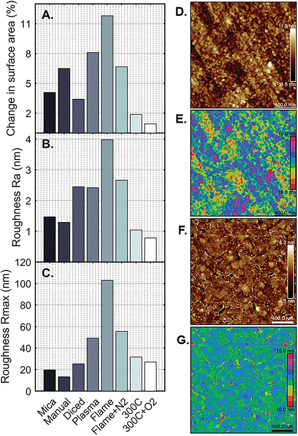
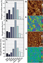
Figure 6 Surface roughness of processed gold films. A) Percent difference in surface area of 2 μm x 2 μm AFM scan from 4 μm2 on gold films with differential processing. B) Quantitative roughness measurement of height deviation average from flattened image (Ra) in the same AFM images. C) Maximum feature height in flattened AFM images (Rmax). Samples shown are (from left to right): cleaved mica; manually-cut Si/SiO2; diced Si/SiO2 wafer; diced Si/SiO2 with 5 min oxygen plasma; diced Si/SiO2 annealed in a gas flame; diced Si/SiO2 annealed in gas flame with nitrogen gas stream; diced Si/SiO2 annealed at 300∘C in forming gas for 21 h; diced Si/SiO2 annealed similarly with 5 min oxygen plasma both before and after annealing. Detailed process notes can be found in Table 3. D–G) 2 μm x 2 μm AFM scans of representative surfaces. D) Titanium (1 nm) and gold (200 nm) are deposited on a clean Si/SiO2 wafer, diced using a dicing saw, and imaged directly after (“Diced” in A–C). Height scale ±11.5 nm. E) Threshold-processed micrograph reproduction of D with 2.5 nm height steps to illustrate surface levels. F) Titanium (1 nm) and gold (200 nm) are deposited on a clean Si/SiO2 wafer, diced using a dicing saw, annealed in forming gas at 300∘C for 21 h, and cleaned afterward for 5 min in a tabletop oxygen plasma tool. Samples were imaged directly after (“300∘C + O2” in A–C). Height scale ±4.3 nm. G) Threshold-processed micrograph reproduction of F with 2.5 nm height steps to illustrate surface levels. AFM images taken on a Dimension Icon AFM (Bruker). Data analysed using NanoScope Analysis software (Bruker).
5.2.2 Dicing methods
To validate a high-throughput, batch deposition process, we compare the roughness of films grown on cleaved mica, Si/SiO2 wafers cut manually with a diamond knife, and Si/SiO2 wafers cut using an auto-dicing saw found in many cleanrooms (e.g., DAD3220, Disco Corporation, Santa Clara, CA USA). The use of a dicing saw enables highly precise sample cutting, but the process itself involves the spray of deionized water, possible ionization of that water during dicing, and ultimately the deposition of silicon dust onto the gold surface. The samples themselves show more visible dust in a light microscope, but AFM imaging demonstrates only slight increase in surface roughness (2.45 nm to 1.47 nm) and comparable surface area (4.14 μm2 to 4.16 μm2) when contrasted with samples deposited on cleaved mica (Figure 6A–C, Table 3). Surface features have similar phenotype with nodes ∼70 nm in diameter and ∼10 nm in height. Like thin films on cleaved mica, silicon wafers diced using a dicing saw may be appropriately flat for KPFM and break junction experiments but should be subjected to downstream processing for SPM modes that require gain and feedback modulation.
5.2.3 Processing of surfaces after dicing
After deposition of gold on whole wafers and use of the dicing saw, samples can be subjected to additional processing to increase the overall surface homogeneity of the gold film. The primary objectives of downstream processing are to produce grain-like surface features, rather than the rounded nodes produced during deposition, and to decrease the quantitative surface roughness to produce the best imaging substrate. Flame annealing, as suggested by various sources [30, 31], proved to be an effective method for producing grain-like surface features with locally flat areas up to 500 nm (Table 3). Unfortunately, these surfaces demonstrated tall features at the grain boundaries of up to 100 nm without nitrogen gas, or 60 nm when annealed in a two-stage benchtop flame process with a stream of nitrogen. Repeating this process five times did not improve overall flatness (Table S3).
Other procedures such as acid cleaning and sonication were tested and did little to improve the imaging surface (Table S2). We did, however, find that oxygen plasma in a tabletop plasma cleaner (18 W, Harrick) has the effect of smoothing out surface features—in the case of the rounded nodes produced by deposition, the surface of the nodes were made relatively flat, though the size and overall shape was not changed (Figure 6A–C, Table S2). This suggests that oxygen plasma smooths existing surface features but does not change the topography of these features. As such, oxygen plasma may be used to erode any tall features produced during surface processing.
We tested the effects of controlled temperature annealing on the quality of gold films in a controlled furnace with constant application of forming gas (Ar/H2). While gold has a bulk melting temperature of approximately 1000∘C, a thin film will aggregate and cease to act as a surface at much lower temperatures. We found that for a 200 nm gold film with a 1 nm titanium adhesion layer on Si/SiO2, the denaturation temperature is roughly 400∘C (Table S1). To test the effect of low temperature annealing, gold films were subjected to a temperature of 300∘C in forming gas and annealed for 21 h. The results demonstrate that surface flatness is lowest in samples annealed at 300∘C and cleaned with oxygen plasma both before and after annealing. Compared with unprocessed gold films, these samples exhibited a 70% overall reduction in area roughness (4.04 μm2 to 4.16 μm2) and line roughness (Ra 0.78 nm to 2.45 nm), and comparable maximum feature height (27.1 nm to 25.3 nm) (Table 3, Figure 6A–C). Surface phenotypes assayed with AFM show ∼400 nm grains with ∼5 nm boundary features in annealed samples (Figure 6F–G), compared with ∼70 nm wide nodes with ∼10 nm edge features on unprocessed gold (Figure 6D–E). In sum, the slow anneal at 300∘C appears to provide enough energy for gold atoms to migrate but insufficient energy for the formation of large clusters and surface degradation. Slow annealing has the overall effect of producing flat surface grains that are ideal for SPM imaging.
6 Gold Protocol: Atomically-flat Imaging Substrates
6.1 Cleaning the Surface and Depositing Gold
The purpose of surface cleaning on Si/SiO2 wafers is to etch away any dust that may have been deposited on the surface in order to reduce the substrate to an atomically-flat crystal. The use of piranha solution allows for a thorough cleaning of surface dust, but it is also hazardous to the researcher. Piranha is highly exothermic and an aggressive oxidizer. Use extreme care when formulating and make note of the exact time when the acid is formulated as its potency diminishes over a matter of hours. Pre-deposition oxygen plasma is a recommended but optional step, depending on whether a wafer can fit inside the given plasma cleaner. In general, oxygen plasma will remove organic residues, and, at relatively low power (18 W), cleaning should occur for at least three minutes, but can continue for any reasonable amount of time.
- Prepare piranha solution in an acid-safe fume hood by slowly adding one part (10 mL) hydrogen peroxide (H2O2) to three parts (30 mL) concentrated sulfuric acid (H2SO4) in a glass dish that can fit your silicon wafer. Cover with perforated aluminum foil and label with caution markers and the time of mixing. Use extreme caution as the dish will be quite hot.
- Allow the piranha solution to age for 90 min. The glassware should be warm but no longer hot.
- While the piranha is aging, prepare two glass dishes, one with 40 mL deionized water, the other with 40 mL ethanol.
- Using acid-safe tweezers, place the silicon wafer in the piranha solution and leave it for 5 min to clean.
- Remove the wafer carefully from piranha and wash briefly in distilled water, then in ethanol.
- Blow wafer dry in an inert gas such as H2, N2 or Ar, letting the gas stream blow toward the tweezers. Store in an airtight container.
- Safely dispose of the piranha solution in an appropriately-labeled, acid-safe waste container.
- Clean wafer in oxygen plasma for 5 min (optional).
- Deposit 1 nm titanium (0.5 Å/s) followed by 200 nm gold (0.5 Å/s) using a cleanroom deposition chamber.
6.2 Processing the Gold Surface
The purpose of surface processing is to reduce the surface roughness of the gold film that is acquired during deposition, during dicing, and by passive exposure to air, as discussed above. Some dicing saws will use adhesive tape to keep a wafer in place, which will require peeling off samples by hand. To the extent possible, use tweezers for this process and avoid making any contact between a gloved hand and the center of the imaging surface, as this will irreparably contaminate the gold substrate.
- Cut the wafer into 1 cm2 squares using a cleanroom dicing saw. Store in airtight container until individual surfaces are needed.
- Remove individual samples from diced wafer using tweezers in cleanroom environment.
- Clean samples in tabletop plasma sterilizer (18 W) for 5 min.
- Anneal samples in forming gas (Ar/H2) for 21 h at 300∘C.
- Again, clean samples in tabletop plasma sterilizer (18 W) for 5 min.
- Store in an airtight container and use the surface for imaging within 48–72 h.
6.3 Depositing the DNA Nanowires
In order to control for the effects of buffer salts on single-molecule conductivity, DNA samples may be filtered into deionized water. STM break junction experiments on DNA have been performed on surfaces with both in buffer salt fluid as well as deionized water, and it is left to the discretion of the researcher whether this is a necessary step. DNA is not fully stable in salt-free solutions; therefore, after performing a buffer exchange, the sample should be deposited on an imaging surface as soon as possible to avoid degradation. In this protocol, we do not perform buffer exchange, but rather wash the imaging surface in deionized water after deposition of the DNA in order to remove residual salt. Samples producing images will need to have the solution concentration tailored to the image results—if messy, aggregated DNA is observed on the imaging substrate, consider dilution up to 100x in nuclease-free water reduce surface density of DNA. An initial sample may use undiluted DNA or 2–5x dilution as a first guess.
- Clean the surface in tabletop plasma sterilizer (18 W) for 3–5 min in order to remove any dust and increase adhesiveness of the surface.
- Within 30 s of removing from plasma cleaner, deposit 5 μL DNA sample in the center of the surface. Cover and set aside on the bench to allow the water (5–10 min).
- Wash surface by pipetting 10 μL nuclease-free water onto the surface. Wait 30–60 s and slowly wick the water off the edge of the imaging surface with a sterile cloth or wipe.
- Wash up to twice more, depending on surface salt density, as seen in the light microscope in your SPM. The surface should appear less dirty to the naked eye or under an optical microscope.
6.4 Single-Molecule Electronics Application
The sample may now be imaged or assayed via the SPM method of choice. In order to prepare the sample for imaging, the surface will have to be electrically connected to the SPM stage using conductive silver paint or copper tape.
- Apply conductive silver paint to edge of sample to create a continuous region of conductive glue between the gold surface and the silicon underside of the chip. Allow the paint to dry.
- Using metal tweezers, transfer the sample to the SPM stage and apply chuck vacuum to reduce vibration.
- Perform SPM measurement of choice.
7 Conclusions
Metallic DNA nanowires are of interest to the field of molecular electronics and self-assembled nanosystems. Here we present an effective protocol for synthesizing such constructs and preparing imaging substrates on conductive films. With some thought to the downstream application, a binding mechanism and reaction buffer can be selected to facilitate efficient annealing and measurement. Furthermore, with consideration to the single-molecule assay, a gold surface process can be chosen to facilitate atomic resolution and molecular conductance analysis. We expect that a detailed and reproducible method for DNA nanowire synthesis will allow for more complex exploration of sequence design, behavior and geometry. This protocol can ultimately be used to prepare samples for a variety of experiments in the field of molecular electronics, including nanoelectrode or nanogap measurement [5, 31]; scanning probe [32] and break junction experiments [7, 10]; and ultimately, perhaps, the fabrication and assessment of logic devices for nanoelectronics.
Acknowledgements
The authors wish to thank Professor Gary Wessel of Brown University for extensive creative discussion to begin this work, as well as assistance in getting it off the ground while it was an aspirational iGEM project. We further thank James Hone and his students for the use of their annealing furnace. This work was funded by a NASA Space Technology Research Fellowship to S.V.
References
[1] E. Braun, et al. ‘DNA-templated assembly and electrode attachment of a conducting silver wire’, Nature, 391(6669):775–778, 1998.
[2] L. Montagnier, et al. ‘Electromagnetic signals are produced by aqueous nanostructures derived from bacterial DNA sequences’, Interdisciplinary Sciences: Computational Life Sciences, 1(2):81–90, 2009.
[3] A. Storm, et al. ‘Insulating behavior for DNA molecules between nanoelectrodes at the 100 nm length scale’, Applied Physics Letters, 79(23):3881–3883, 2001.
[4] A. Y. Kasumov, et al. ‘Proximity-induced superconductivity in DNA’, Science, 291(5502): 280–282,2001.
[5] G. I. Livshits, et al. ’Long-range charge transport in single G-quadruplex DNA molecules’, Nature Nanotechnology, (9): 1040–1046, 2014.
[6] L. Xiang, et al. ‘Intermediate tunnelling–hopping regime in DNA charge transport’, Nature Chemistry, 7(3):221–226, 2015.
[7] L. Venkataraman, et al. ‘Dependence of single-molecule junction conductance on molecular conformation’, Nature, 442(7105):904–907, 2006.
[8] C. Bruot, et al. ‘Effect of mechanical stretching on DNA conductance’, ACS Nano, 9(1):88–94, 2014.
[9] B. Xu, et al. ‘Direct conductance measurement of single DNA molecules in aqueous solution’, Nano Letters, 4(6):1105–1108, 2004.
[10] E. Toomey, et al. ‘Comparison of Canonical versus Silver(I)-Mediated Base-Pairing on Single Molecule Conductance in Polycytosine dsDNA’, Journal of Physical Chemistry C, 120(14):7804–7809, 2016.
[11] H. Torigoe, et al. ‘Thermodynamic and structural properties of the specific binding between Ag(+) ion and C:C mismatched base pair in duplex DNA to form C-Ag-C metal-mediated base pair’, Biochimie, 94(11):2431–2440, 2012.
[12] Y. Miyake, et al. ‘MercuryII-mediated formation of thymine-HgII-thymine base pairs in DNA duplexes’, Journal of the American Chemical Society, 128(7):2172–2173, 2006.
[13] S. Johannsen, et al. ‘Solution structure of a DNA double helix with consecutive metal-mediated base pairs’, Nature Chemistry, 2(3):229–234, 2010.
[14] G. H. Clever, M. Shionoya, ‘Metal-base pairing in DNA’, Coordination Chemistry Reviews, 254(19–20): 2391–2402, 2010.
[15] V. B. Pinheiro, P. Holliger, ‘Towards XNA nanotechnology: new materials from synthetic genetic polymers’, Trends in Biotechnology, 32(6):321–328, 2014.
[16] H. Yamaguchi, et al. ‘The structure of metallo-DNA with consecutive thymine-HgII-thymine base pairs explains positive entropy for the metallo base pair formation’, Nucleic Acids Research, 42(6):4094–4099, 2014.
[17] S. S. Mallajosyula, S. K. Pati, ‘Conformational tuning of magnetic interactions in metal–DNA complexes’, Angewandte Chemie, 121(27):5077–5081, 2009.
[18] S. Roche, ‘Sequence dependent DNA-mediated conduction’, Physical Review Letters, 91(10):108101, 2003.
[19] S. S. Mallajosyula, S. K. Pati, ‘Toward DNA conductivity: a theoretical perspective’, The Journal of Physical Chemistry Letters, 1(12):1881–1894, 2010.
[20] H. Torigoe, et al. ‘Thermodynamic properties of the specific binding between Ag+ ions and C:C mismatched base pairs in duplex DNA’, Nucleotides, Nucleosides and Nucleic Acids, 30:149–167, 2011.
[21] S. M. Swasey, et al. ‘Silver (I) as DNA glue: Ag+-mediated guanine pairing revealed by removing Watson-Crick constraints’, Scientific reports, 5: 10163, 2015.
[22] L. Venkataraman, et al. ‘Single-molecule circuits with well-defined molecular conductance’, Nano Letters, 6(3):458–462, 2006.
[23] A. Ono, et al. ‘Specific interactions between silver(I) ions and cytosine-cytosine pairs in DNA duplexes’, Chemical Communications (Cambridge), (39):4825–4827, 2008.
[24] N. Peyret, et al. ‘Nearest-neighbor thermodynamics and NMR of DNA sequences with internal A.A, C.C, G.G, and T.T mismatches’, Biochemistry, 38(12):3468–3477, 1999.
[25] R. Owczarzy, et al. ‘Predicting stability of DNA duplexes in solutions containing magnesium and monovalent cations’, Biochemistry, 47(19):5336–5353, 2008.
[26] J.-L. Leroy, et al. ‘Intramolecular folding of a fragment of the cytosine-rich strand of telomeric DNA into an i-motif’, Nucleic Acids Research, 22(9):1600–1606, 1994.
[27] C. M. Ritchie, et al. ‘Ag nanocluster formation using a cytosine oligonucleotide template’, Journal of Physical Chemistry C, 111(1):175–181, 2007.
[28] H. T. Allawi, J. SantaLucia, ‘Thermodynamics and NMR of internal G⊙ T mismatches in DNA’, Biochemistry, 36(34):10581–10594, 1997.
[29] C. Nogues, M. Wanunu, ‘A rapid approach to reproducible, atomically flat gold films on mica’, Surface Science, 573(3): L383-L389, 2004.
[30] U. Maver, et al. ‘Preparation of Atomically Flat Gold Substrates for AFM Measurements’, Acta Chimica Slovenica, 59(1), 2012.
[31] T. Someya, et al. ‘Alcohol vapor sensors based on single-walled carbon nanotube field effect transistors’, Nano Letters, 3(7):877–881, 2003.
[32] D. Zikich, et al. ‘I-Motif Nanospheres: Unusual Self-Assembly of Long Cytosine Strands’, Small, 7(8):1029–1034, 2011.
Biographies

Simon Vecchioni received his B.S. in Biology from Brown University in 2013. That same year he joined the laboratory of Lynn Rothschild at NASA Ames Research Center to investigate the biosynthesis of electronic materials. After moving to Columbia University in New York to pursue a Ph.D. in Biomedical Engineering, he joined the group of Shalom Wind to focus on nanoscale self-assembly and DNA nanotechnology. Since 2014, he has been supported by a NASA Space Technology Research Fellowship and has continued to pursue work on DNA nanoelectronics with the support of Wind and Rothschild.

Mark C. Capece earned a B.S. in Chemistry and Physics from the University of Louisville in 2011, where his honors thesis demonstrated the practical lumped-element design of a magic angle spinning triple-resonance solid-state NMR probe. He then received a Ph.D. in Chemistry from Stanford University in 2018. His graduate work used solution NMR and single-molecule fluorescence to model functional mRNA structures that regulate translation. Capece’s research interests continue to focus on NMR technology development and biological applications.

Emily Toomey received her Sc.B. in Electrical Engineering from Brown University in 2015, where she studied the electrical characterization of DNA in the laboratory of Prof. Jimmy Xu. She had previously interned at the NASA Ames Research Center under Dr. Lynn Rothschild in 2013, where she explored the modification of DNA structures by metal ion intercalation in collaboration with Simon Vecchioni. Emily has been pursuing a Ph.D. in Electrical Engineering from the Massachusetts Institute of Technology since 2015. Her current work under Prof. Karl K. Berggren focuses on superconducting nanoelectronics and nanofabrication.

Lynn Rothschild is passionate about the origin and evolution of life on Earth or elsewhere, while at the same time pioneering the use of synthetic biology to enable space exploration. She is a senior scientist NASA’s Ames Research Center, as well as Adjunct Professor at Brown University. Since 2011 she has been the faculty advisor of the award-winning Stanford-Brown iGEM team, which has pioneered the use of synthetic biology to accomplish NASA’s missions, focusing on the human settlement of Mars, astrobiology and such innovative projects as BioWires, making a biodegradable UAS (drone) and using fungal mycelia as a building material. She is a fellow of the Linnean Society of London, The California Academy of Sciences and the Explorer’s Club.

Shalom J. Wind received his Ph.D. in Physics from Yale University in 1987. Following his doctoral studies, he worked at IBM’s Thomas J. Watson Research Center, focusing primarily on nanoelectronic devices. He moved to the Department of Applied Physics and Applied Mathematics at Columbia University in 2003. Wind’s present research focuses on molecular-scale fabrication and the interface between biological and technological materials and systems.
Journal of Self-Assembly and Molecular Electronics, Vol. 6_1, 61–90.
doi: 10.13052/jsame2245-4551.6.004
This is an Open Access publication. © 2019 the Author(s). All rights reserved.