Characterization of Emergence
of the Coulomb Blockade
in a Pearl-Like DNA-AuNP Assembly
Kosti Tapio and J. Jussi Toppari
University of Jyvaskyla, Department of Physics, Nanoscience Center, P.O. Box 35, FI-40014 University of Jyväskylä, Finland
E-mail: kosti.t.o.tapio@jyu.fi; j.jussi.toppari@jyu.fi
Received 31 January 2017; Accepted 9 August 2017;
Publication 29 August 2017
Abstract
Due to its superior self-assembly properties and vast functionalization possibilities DNA has long been one of the most promising candidates for fabrication of nanoscale electrical components using molecular building blocks. There exist already many demonstrations on optical devices based on organizing metallic nanoparticles (NP) via DNA self-assembly, but despite the promises only few DNA based electrical devices or studies have been realized so far. Here we study the gold NP conjugated and metallized DNA TX-tile-structure, which we recently showed to exhibit the room temperature Coulomb blockade, the pre-requisition for a single electron transistor. The properties of the obtained Coulomb blockade are further characterized via the differential conductance measurements at temperatures ranging from 4.2 K to 10.2 K. The results show sharp blockade plateaus with varying threshold voltages, which yields further evidence of a gating effect by background charges. This strongly indicates that the DNA-NP assembly functions as a single electron transistor. Also, the additional growth of gold NPs and electrodes via chemical gold deposition process, needed to achieve the Coulomb blockade, is studied here in more details, yielding more insight to the process, and thus helping to realize better control of it.
Keywords
- DNA
- gold nanoparticles
- metallization
- single electron transistor
- differential conductance
1 Introduction
The fabrication of nanoscale electrical components using molecular building blocks has greatly intrigued researchers due to the seen possibilities in overcoming the difficulties of semiconductor technology in producing ever-diminishing nano- and microelectronics components demanded by the industry [1]. Fabrication of such components, already nearing the molecular scale, is complex and costly by conventional methods [2, 3], while the bottom-up fabrication using molecular tools can offer a relatively cheap alternative.
For this, one of the most promising candidates has been DNA due to its programmable self-assembly and vast functionalization possibilities [4–6]. Many different shapes had been formed out of DNA, e.g., holiday junctions [7], double crossover tile (DX-tile) [8] and triple crossover tile (TX-tile) [9], until the discovery of DNA origami in 2006 [10], which enabled fabrication of almost any arbitrary shaped 2D- or 3D-structures [11, 12]. Since then, DNA origami have been utilized as, e.g., nanobreadboards [13], enzyme reactors [14], nanotweezers [15, 16] and drug carriers [17].
For electronics, the most promising property of DNA origami is its capability to act as a platform to organize nanoparticles (NP) [18] or other electrical building blocks [19]. Also direct metallization of origami to form nanoscale wires and other metallic shapes has been investigated widely [20], but this approach does not provide an easy way to produce functional electronic devices. Many groups have demonstrated optical devices based on organizing metallic NPs exhibiting localized surface plasmon resonance [21–24], but despite the promises only few DNA based electrical devices or studies have been realized [19, 25–27].
One of the most interesting components, which could be fabricated using DNA and metallic NPs, is the single electron transistor (SET) [28], which can be utilized, e.g., as an extremely sensitive electrometer [29], single electron pump for a quantum current standard [30], or as a Coulomb blockade thermometer [31]. However, a severe downside of most SET devices is their requirement for cryogenic temperatures. Recently, we have demonstrated a TX-tile based DNA platform functionalized with three gold nanoparticles (AuNP) exhibiting the Coulomb Blockade, the prerequisite for the SET operation, up to room temperature [32].
Here we further investigate these TX-tile-AuNP conjugated nanoassemblies forming the SET. One of the crucial issues in fabrication of SETs is the control of the transparency of the tunneling barriers. In earlier studies the space between the metallic NPs has been too large or uncontrolled to enable sufficient tunneling [26, 27]. To tackle this, we utilized precise attachment of AuNPs combined with a subsequent expansion of them [32] by the same chemical metallization process, which has been used to produce metallic nanowires [27]. However, the essential chemical expansion process is hard to control within the needed precision. Here, we aim to improve our method by carrying out more detailed analysis on how the metallization process affects the electrical properties of the assembly. This yields insight into the amount of expansion needed for the Coulomb blockade to appear without short-circuiting of the sample due to connected islands and electrodes, which also happens often. In addition, we characterize electrical properties of the best device in more detailed way than in Reference 32, by measuring its differential conductance curves at several low temperatures. These results show even more clearly the observed blockade and the variations in the threshold voltage due to sudden changes in the background charges [33].
2 Experimental Procedures
2.1 Fabrication and Dielectrophoretic Trapping of TX-tile-AuNP Assemblies
All the oligonucleotides were purchased from Integrated DNA technologies (IDT, Coralville, Iowa, USA). The TX-tile-AuNP assemblies were fabricated and trapped between fingertip electrodes using methods reported earlier [32, 34]. In short, the solution containing TX-tileB – TX-tileA – TX-tileB structures (BAB) was mixed with two solutions each containing AuNPs with different complementary DNA strands that attach either to tile A or tile B. The mixing ratio was BAB : AuNPA : AuNPB = 1 : 1 : 2. Then the mixture was heated to 65∘C and slowly cooled down to room temperature. Finally, the free sticky ends of the B tiles were functionalized with oligos having thiols to secure attaching to the gold electrodes, i.e., three thiols at both ends of the BAB complex (see Figure 1A). Trapping of the structure between nanoscale gold electrodes fabricated by e-beam lithography was carried out as explained in our earlier works [32, 34]. We verified the successful trapping of BAB-AuNP assemblies by AFM imaging in tapping mode in air using Digital Instruments Dimension 3100 atomic force microscope, since methods like scanning electron microscopy would contaminate the sample before any electrical measurements or gold enhancement. We used Nanosensors aluminum coated, tapping mode tips (PPP-NCHR) with the tip radius below 10 nm and the resonance frequency of 330 kHz.
2.2 Metal Enhancement of TX-tile-AuNP Assemblies
The gold parts of the trapped TX-tile-AuNP assemblies were expanded using gold enhancement kit (Nanoprobes, Yaphank, New York, USA) along the manufacturer’s instructions, with the exception that the enhancer and the initiator solutions were diluted 12 times and incubation time was 30 s. For slower growth rate, a small amount of 5–10 nm in diameter AuNPs were added to the gold enhancement solution to offer competing reduction surfaces to slow down the growth rate of the electrode structure and the trapped assemblies. See Section 3 Results for more details.
2.3 IV-Characterization and the Differential Conduction Measurement
For the current-voltage (IV) measurements we used Stanford Research Systems SR560 voltage preamplifier and Stanford Research Systems SR570 current preamplifier. In the differential conductance measurements, the AC-voltage and -current were measured using Stanford Research System Model SR830 DSP Lock-in Amplifiers. For the AC-measurement, the AC- and DC-signals were generated and combined by a home-made programmable voltage source controlled by Labview program (National Instruments). Readings of the electrical measurements were recorded on a computer equipped with National Instruments NI PXI-6251 multifunction data acquisition card.
In room temperature (RT) measurements of the trapped samples, the fingertip electrodes were connected to a self-made sample holder with co-axial output cables by pressing two metal needles to the contact pads of the electrodes. The holder together with the TX-tile-AuNP assembly was placed inside an electrically shielded box, and the output cables were connected to measurement electronics via feedthroughs of the box. Subsequently, the IV-characteristics were measured by applying a stepwise increasing DC-voltage while recording the current. After each voltage changes the sample was let to stabilize for 500 ms before recording the current. For the low temperature measurements, we placed one of the samples into a home-made sample stage at the end of the long rod with all the measurement wirings inside, i.e. a dipstick. The contacts were established by bonding aluminum wires between contact pads of the dipstick and the fingertip electrodes using F&K Delvotec 5430 bonder (Bondtechnik GmbH, Ottobrunn, Germany). The dipstick was equipped with Cernox CX-1030 thin film temperature sensor (Lake Shore Cryotronics, Westerville, Ohio, USA) for precise temperature reading. First, the stick was dipped in liquid nitrogen for intermediate cooling and subsequently into a cryogenic dewar containing liquid helium (4.2 K). The temperature gradient above helium inside the dewar was exploited to alter the temperature of the sample between 4.2 K and 10.2 K.
For the differential conductance measurements we used sinusoidal 4 mV peak-to-peak AC-voltage at 13 Hz. The differential voltage across the sample was measured via a voltage preamplifier feeding the lock-in amplifier. The preamplifier had 3–100 Hz bandpass filter to provide noise prefiltering. Similarly, the differential current was measured by putting a current preamplifier in series with the sample and connecting its voltage readout to a lock-in amplifier. The sensitivity of the current amplifier was 10-9A/V. Sensitivities of both of the lock-in amplifiers were 100 mVmax and the time constants were 3 s. The DC-bias voltage was measured simultaneously by a voltage preamplifier equipped with a 3 Hz low pass filter to discard the AC-excitation. Both voltage preamplifiers had 6 dB attenuation slope in filtering.
3 Results
3.1 Chemical Gold Growth of TX-tile-AuNP Assemblies
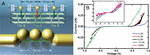
This work utilizes well-studied DNA structure [34], which contains two distinctly different TX-tiles tiles (see Figure 1A), where either 6 (tile A) or 7 (tile B) unique single stranded DNA (ssDNA) fold together to form three parallel, interconnected double stranded DNA (dsDNA) helixes [9]. The middle tile A has 180∘ rotational symmetry, so that the tile B can bind to the both sides of it via three sticky ends with the lengths of 8 nucleotides, thus forming a TX-tileB – TX-tileA – TX-tileB tile assembly or BAB in short. This way the length is also limited to only three TX-tiles. In addition to the sticky ends binding the tiles together, each tile includes a sticky end in the middle to attach a AuNP functionalized with ssDNA strands complementary to the sticky end. The conjugated BAB-AuNP assembly with three AuNPs on a row and thiol functionalizations at both ends (see Section 2.1), was subsequently trapped between fingertip electrodes using dielectrophoresis [35], and electrically characterized at different temperatures ranging from 4.2 K to RT. Figure 2A and 2B show the electrodes of sample 1 before and after the successful trapping. As we have demonstrated, this BAB-AuNP assembly does not exhibit the Coulomb blockade as such because of suppressed tunneling due to too large gaps between the AuNPs [32].
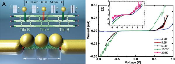
Figure 1 (A) A schematic picture and an artistic 3D view of the BAB-AuNP assembly. The dark green and red strand sticking out of the schematic structure represent the two different sticky ends with AuNPs attached with complementary DNA strands. The capacitances C represent the capacitances of the tunneling gaps between the AuNPs and outside electrodes. (B) IV-characteristics of one of the BAB-AuNP assemblies showing the Coulomb blockade, measured at temperatures from 4.2 K to room temperature.
Since we observed no Coulomb blockade for the trapped BAB-AuNPs assemblies, but only an insulating behavior with resistances in the range of tera-Ohms, extra process of chemical gold growth were carried out for the trapped samples using a gold enhancement kit (as described in Section 2.2). After this, we observed a clear Coulomb blockade for several samples (see Figure 1B) [32]. As a negative control we have applied the same gold enhancement process to a trapped plain BAB assembly, which rarely yielded Coulomb Blockade or any conductivity, as shown in Figures S6 and S7 in Reference 32.
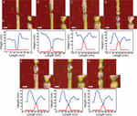
We carried out the chemical extension process of the gold in several steps. After the first step with faster growth, we observed roughly 10–15 nm growth of the gold structures (also electrodes) as shown in Figure 2C. On the same procedure, the smooth features of the original structure got much more granular. This is quite typical for the gold salt reduction reaction on metallic nanostructures [20]. Since the Coulomb blockade was still not observed after the initial gold growth, we adopted a second gold growth step with the growth rate tuned slower by introducing 5–10 nm AuNPs to the solution during the reduction reaction to supply competing reduction sites and thus slowing down the growth rate of the trapped BAB-AuNP assembly. We repeated this slow growth step as many times as needed until the Coulomb blockade or sometimes low resistance Ohmic behavior, due to connected metallic parts, was observed. The average height increase was roughly 0.5–3 nm after each step (Figures 2D–G).
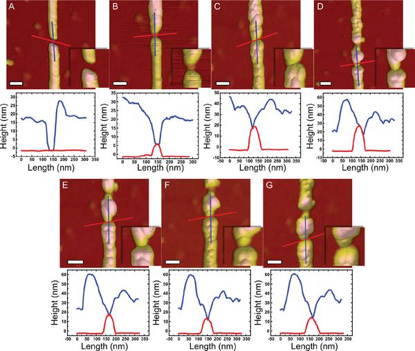
Figure 2 AFM images of the gold growth process for the sample 1 together with height cross-sections along the marked red and blue lines. (A) The empty electrode structure before trapping. (B) The trapped BAB-AuNP assembly. (C)–(G) The same trapped BAB-AuNP assembly after 1st and all the way to 5th gold growth step. The insets present the zoom of the gap region. The scale bars are 100 nm.
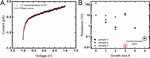
After each growth step, we measured the IV-characteristics of the sample again. Before observation of the Coulomb blockade, samples showed a linear resistance combined with clear charging effects due to the capacitive gaps, as shown for the sample 1 in Figure 3A. We solved the resistance R of the system by fitting the Equation (1), which takes into account the charging currents induced by our stepwise increasing bias voltage, into each IV-curve [36].
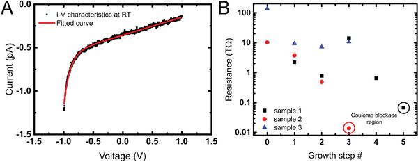
Figure 3 (A) The IV-characteristics of the sample 1 after 2nd gold growth step (black circles) and the fit by Equation (1) (red line). The scanning in this case started from negative voltage towards positive, thus showing higher initial charging current which saturates later. (B) The resistances of the trapped, gold enhanced BAB-AuNP-samples after several gold growth steps. The circulated points mean samples showing a clear Coulomb blockade. In this case the resistance values have been calculated within the Coulomb blockade region.
where I0 is the maximum charging current at the bias transients, α is a constant including the ratio of the stabilization time of the measurement and the time constant of the charging current, n refers to the nth measurement point and Vn is the corresponding voltage. The equation essentially describes a DC-biased capacitive system that has initial charging currents after each change of the bias voltage, i.e., RC-equivalent circuit, which later saturates to a purely resistive behavior following the stepwise increasing DC-voltage. As an example, the fitting for the IV-characteristics of the sample 1 after 2nd gold growth step is illustrated in Figure 3A. We measured similar IV-curves and resolved the resistance R via fitting for all of the samples after all of the gold growth steps. The achieved chi-squared value was in all cases about 10-9. The solved resistances for samples 1–3 are plotted in Figure 3B.
It is evident from the Figure 3B that in general the resistances of the samples drop after each growth step, which is reasonable: the tunneling gaps within the sample are getting smaller and thus the tunneling current is increasing and resistance decreasing. The initial larger drop is due to the bigger growth step, and subsequently the slower growth rate will induce smaller resistance changes. The sample 1 has increase in the resistance after 3rd growth, but this is due to dislodged part along the electrode structure, resulting in higher resistance, as visible in Figure 2. This most probably happened right after the second resistance measurements as the AFM image taken after that (Figure 2D) already shows the damaged fingertip electrode.
The point, when the tunneling barriers are small enough for a significant current, is hard to predict exactly from the resistance vs. growth step curves, but it seems that at least 2–4 growth steps with slower rate after the faster initial growth were required to achieve the Coulomb blockade. There were also samples, that initially seemed to grow well, i.e., the resistance decreased, but ultimately after few steps were unsuccessful due to breaking down during the measurement. This happens most probably because the chemical expansion process connects the metallic parts thus short-circuiting the sample, which subsequently leads to too high current. The sample 3, which broke after the 3rd step, is a good example of this. Interestingly enough, the resistance has not significantly increased although the whole electrode structure has dislocated.
3.2 Differential Conductance Characterization of a Gold Enhanced BAB-AuNP Assembly
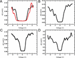
We performed also differential conductance measurements for the sample 1. After cooling it down in liquid nitrogen, the sample was placed inside a dewar with liquid helium and let cool down to 4.2 K, where IV-characteristics (see Figure 1B) and the differential conductance curves (Figure 4) were measured. The temperature was changed by exploiting the temperature gradient inside the dewar by raising the sample above the liquid helium level. Both IV-characteristics and differential conductance curves were measured at four different temperatures: 4.2 K, 5.2 K, 5.9 K and 10.2 K as shown in Figures 1B and 4. All the conductance curves show a sharp and clear plateau with conductance closing to zero, which indicates the Coulomb blockade region. The fluctuations of the conductance outside the blockade region can be due to different tunneling resistances at different junctions [28], or due to electronic states within single NP.
The Coulomb blockade threshold voltages Vth, after which the measured assembly starts to conduct well, are listed in Table 1 at different temperatures. The threshold voltages differ between the measurements at different temperatures, but also between two consecutive measurements at 4.2 K (black and red curves in Figure 4A). Since the temperature is constant during these measurements, the only other effect that can cause this change is the alteration in the gate voltage. Even though we did not fabricate any gate electrode, this effect suggests that the device effectively functions as a SET with moving background charges acting as a gate voltage. This effect of moving background charges is well recognized in the field of single electron devices [28, 33]. Due to the same reason the threshold varies between the measurements at different temperatures. This reasoning becomes even more evident from the Figure 1B which shows clear jumps on the IV-curves due to the rapid changes in the background charges, especially since these jumps happen more often at higher temperatures where excess charges get more energy to move.
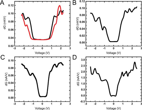
Figure 4 The differential conductance of the sample 1 at temperature of (A) 4.2 K, (B) 5.2 K, (C) 5.94 K and (D) 10.2 K. The plateau, i.e. the Coulomb blockade region, at 4.2 K differs for two subsequent measurements (red and black curves), and also within other temperatures. This is most probably due to changes in the background charges, as explained in the text.
Table 1 The threshold voltage of the sample 1 at different temperatures
| Temperature (K) | Negative Threshold Voltage (V) |
Positive Threshold Voltage (V) |
| 4.2 |
–1.0 | +0.76 |
| 4.2 |
–1.2 | +0.88 |
| 5.2 | –0.48 | +0.48 |
| 5.94 | –0.31 | +0.48 |
| 10.2 | –0.35 | +0.28 |
4 Discussion and Conclusion
We have demonstrated how to achieve the Coulomb blockade within the previously studied DNA structure conjugated with three nanoparticles [32], and performed low temperature differential conductance measurements to further characterize it. Initially, as described in our previous work, the trapped BAB-AuNP assemblies did not exhibit any kind of single electron tunneling behavior due to too large gaps between the AuNPs. So, we utilized chemical gold growth steps to reduce the gap size. This was done by adopting a faster initial growth step followed by series of growth steps with slower growth rate for fine tuning. The steps resulted in 10–15 nm and 0.5–3 nm growth on the gold structures, respectively. Typical end-result was a granular structure, which is quite characteristic for chemical reduction reactions on a nanostructure with multiple seeding locations. Also, the slower growth process involved separate small, 5–10 nm in diameter gold nanoparticles to reduce the growth process, which could have increased the granularity of the samples. Fortunately, it seems that the overall roughness does not significantly increase from the initial growth.
To characterize the gold growth steps and especially the point to achieve the Coulomb blockade, we performed resistance analyses by fitting the IV response of a stepwise RC-equivalent circuit (Equation 1) to the measured IV-characteristics having a low conductivity. It was discovered, that the formation of the Coulomb blockade in the BAB-AuNP assemblies required several gold growth steps. In all of the cases, when the blockade was achieved, the resistance within the blockade region was few tens of MΩ, which is significantly lower than the starting point of few TΩ. This kind of growth process might be challenging or even impractical to realize in any industrial fabrication process. However, the results of the resistance analysis yielded information of the amount of required gold expansion, e.g., for realizing a one-pot gold growth process to fabricate SET out of DNA structures while monitoring the resistance.
The differential conductance measurements reveal a very clear and relatively sharp dip in the conductance with a plateau, which is a further confirmation of the existence of the Coulomb blockade. We observed that consecutive differential conductance measurements at the same temperature produced different threshold voltages. Since the only true factor to influence the threshold voltage is the gate voltage, the differences in the threshold voltages mean most probably that there are some background charge fluctuations happening that alter the gate voltage of the system, which was already speculated in the previous article, but now more clearly evident via the conductance measurements. This is further assuring that the gold enhanced BAB-AuNP assembly is indeed functioning as SET.
Acknowledgments
The work has been financially supported by Academy of Finland (Projects 263526, 130900, 218182, 263262).
References
[1] M. Ratner. Nat. Nanotechnol., 8, 378–381 (2013).
[2] N. Mojarad, J. Gobrecht, and Y. Ekinci. Microelectron. Eng., 143, 55–63 (2015).
[3] Y. S. Rusli, and N. Singh. IEEE Trans. Nanotechnol., 10, 96–98 (2011).
[4] A. V. Pinheiro, D. Han, W. M. Shih, and H. Yan. Nat. Nanotechnol., 6, 763–772 (2011).
[5] O. I. Wilner, and I. Willner, Chem. Rev., 112, 2528–2556 (2012).
[6] V. Linko, A. Ora, and M. A. Kostiainen. Trend Biotechnol., 33, 586–594 (2015).
[7] M. L. Petrillo, C. J. Newton, R. P. Cunningham, N. R. Kallenbach, R.-I. Ma and N. C. Seeman. Biopolymers, 27, 1337–1352 (1988).
[8] E. Winfree, F. Liu, L. A. Wenzler, and N. C. Seeman. Nature, 394, 539–544 (1998).
[9] T. H. LaBean, H. Yan, J. Kopatsch, F. Liu, E. Winfree, J. H. Reif, and N. C. Seeman, J. Am. Chem. Soc., 122, 1848–1860 (2000).
[10] P. W.K. Rothemund. Nature, 440, 297–302 (2006).
[11] E. S. Andersen, M. Dong, M. M. Nielsen, K. Jahn, A. Lind-Thomsen, W. Mamdouh, K. V. Gothelf, F. Besenbacher, and J. Kjems. ACS Nano, 2, 1213–1218 (2008).
[12] B. Saccà, and C. M. Niemeyer, Angew. Chem. Int. Ed., 51, 58–66 (2012).
[13] A.-P. Eskelinen, A. Kuzyk, T. K. Kaltiaisenaho, M. Y. Timmermans, A. G. Nasibulin, E. I. Kauppinen, and P. Törmä, Small, 6, 746–750 (2011).
[14] V. Linko, S. Nummelin, L. Aarnos, K. Tapio, J. J. Toppari, and M. A. Kostiainen. Nanomaterials, 6, 139 (2016).
[15] B. Yurke, A. J. Turberfield, A. P. Mills Jr, F. C. Simmel, and J. L. Neumann. Nature, 406, 605–608 (2000).
[16] M. Lui, J. Fu, C. Hejesen, Y. Yang, N. W. Woodbury, K. Gothelf, Y. Liu, and H. Yan. Nature Comm., 4, 2127 (2013).
[17] S. D. Perrault, and W. M. Shih. ACS Nano, 8, 5132–5140 (2014).
[18] B. Ding, Z. Deng, H. Yan, S. Cabrini, R. N. Zuckermann, and J. Bokor, J. Am. Chem. Soc., 132, 3248–3249 (2010).
[19] H. T. Maune, S.-P. Han, R. D. Barish, M. Bockrath, W. A. Goddard III, P.W.K. Rothemund, and E. Winfree, Nat. Nanotechnol., 5, 61–66 (2010).
[20] B. Shen, K. Tapio, V. Linko, M. A. Kostiainen, and J. J. Toppari. Nanomaterials, 6, 146 (2016).
[21] E.-M. Roller, L. K. Khorashad, M. Fedoruk, R. Schreiber, A. O. Govorov, and T. Liedl, Nano lett., 15, 1368–1373 (2015).
[22] X. Lan, Z. Chen, G. Dai, X. Lu, W. Ni, and Q. Wang, J. Am. Chem. Soc., 135, 11441–11444 (2013).
[23] M. Pilo-Pais, A. Watson, S. Demers, T. H. LaBean, and G. Finkelstein. Nano Lett., 14, 2099–2104 (2014).
[24] X. Shen, A. Asenjo-Garcia, Q. Liu, Q. Jiang, F. J. García de Abajo, N. Liu, and B. Ding. Nano Lett., 13, 2128–2133 (2013).
[25] G. Maubach, and W. Fritzsche, Nano Lett., 4, 607–611 (2004).
[26] G. Maubach, D. Born, A. Csáki, and W. Fritzsche. Small, 1, 619–624 (2005).
[27] B. Teschome, S. Facsko, T. Schönherr, J. Kerbusch, A. Keller, and A. Erbe. Langmuir, 32, 10159–10165 (2016).
[28] B. L. Altshuler, P. A. Lee, and R. A. Webb. Mesoscopic Phenomena in Solids. Amsterdam: Elsevier, 173–271 (1991).
[29] R. J. Schoelkopf, P. Wahlgren, A. A. Kozhevnikov, P. Delsing, and D. E. Prober, Science, 280, 1238–1242 (1998).
[30] A. Rossi, T. Tanttu, F. E. Hudson, Y. Sun, M. Möttönen, and A. S. Dzurak, J. Vis. Exp., 100, 52852 (2015).
[31] J. P. Kauppinen, K. T. Loberg, A. J. Manninen, J. P, Pekola, and R. A. Vuotilainen. Rev. Sci. Instrum., 69, 4166–4175 (1998).
[32] K. Tapio, J. Leppiniemi, B. Shen, V. P. Hytönen, W. Fritzsche, and J. J. Toppari, Nano lett., 16, 6780–6786 (2016).
[33] A. N. Korotkov. Int. J. Electron., 86, 511–547 (1999).
[34] V. Linko, J. Leppiniemi, S.-T. Paasonen, V. P. Hytönen, and J. J. Toppari. Nanotechnology, 22, 275610 (2011).
[35] H. A. Pohl. J. Appl. Phys., 22, 869–871 (1951).
[36] A. Kuzyk. Molecular devices for nanoelectronics and plasmonics. Ph.D. dissertation, University of Jyväskylä, Jyväskylä.
Biographies

Kosti Tapio graduated from University of Jyväskylä as M.Sc. in experimental physics in 2012 under supervision of then Academic research fellow Dr. Toppari. He continued for his Ph.D studies the same year in the same molecular electronics and plasmonics group, working on DNA based nanoelectronics and plasmonics structures and assemblies. He will defend his Ph.D thesis in 2017.

J. Jussi Toppari is a senior university lecturer (Adjunct professor/Docent) at Department of Physics, Nanoscience Center, University of Jyväskylä, Finland. He received his M.Sc. (1997) and Ph.D. degrees (2003) in experimental physics of superconducting nanostructures in University of Jyväskylä. After that he worked as a senior assistant in a newly formed Nanoscience Center (NSC) and in 2008 he obtained the degree of adjunct professor (docent) and established his own independent research group in NSC. During 2011 he worked as a senior visiting researcher at the Leibniz Institute of Photonic Technology, Jena, Germany. His current research interest is molecular electronics and plasmonics, in particular DNA nanotechnology and strong light matter coupling.
Journal of Self-Assembly and Molecular Electronics, Vol. 1, 31–44.
doi: 10.13052/jsame2245-4551.5.003
© 2017 River Publishers. All rights reserved.